Light emission device with anisotropic properties

a technology of anisotropic properties and light emitting devices, which is applied in the direction of sustainable manufacturing/processing, instruments, and final product manufacturing, etc., can solve the problems of affecting certain aspects of the image, affecting the quality of the image, and directing a lot of effort to optimize the properties of materials, etc., to achieve good and efficient effects

Active Publication Date: 2020-06-02
UNIV GENT
View PDF9 Cites 0 Cited by
  • Summary
  • Abstract
  • Description
  • Claims
  • Application Information

AI Technical Summary

Benefits of technology

[0008]It is an object of embodiments of the present invention to provide a good and efficient outcoupling of an OLED.
[0019]The electron transport layer may be made of a material having a refractive index having a negative anisotropy. It is an advantage of embodiments of the present invention that the outcoupling can be increased by selecting an electron transport layer showing a specific anisotropy in the refractive index resulting in reduced total internal reflectance. It is an advantage of embodiments of the present invention that electron transport layers having suitable optical properties are available on the market or can be manufactured.
[0021]The OLED may further comprise electrodes. Such electrodes may be made of low work function materials. It is an advantage of embodiments of the present invention that the production of charge carriers may be effective. The OLED also may comprise a substrate. Such a substrate may have birefringent properties. It is an advantage of embodiments of the present invention that highly polarized light may be obtained, improving image characteristics such contrast. The anisotropic layers may have an ordinary refractive index of 1.7. It is an advantage of embodiments of the present invention that organic materials with required properties can be easily obtained or manufactured.

Problems solved by technology

In the past, a lot of effort was directed to optimization of the properties of the materials forming the structure.
The outcoupling is then limited by the quality of the substrate patterning, and the costs may increase while negatively affecting certain aspects of the image (for example reducing the viewing angle).
This document may be applied to OLEDs, because the contrast and image stability of displays can be improved, but the outcoupling, although it may be improved in some cases, is difficult to control, the production is costly, complex and difficult to implement in OLEDs, as thin structures are needed.

Method used


Image

  • Light emission device with anisotropic properties
  • Light emission device with anisotropic properties
  • Light emission device with anisotropic properties

Examples


Embodiment Construction

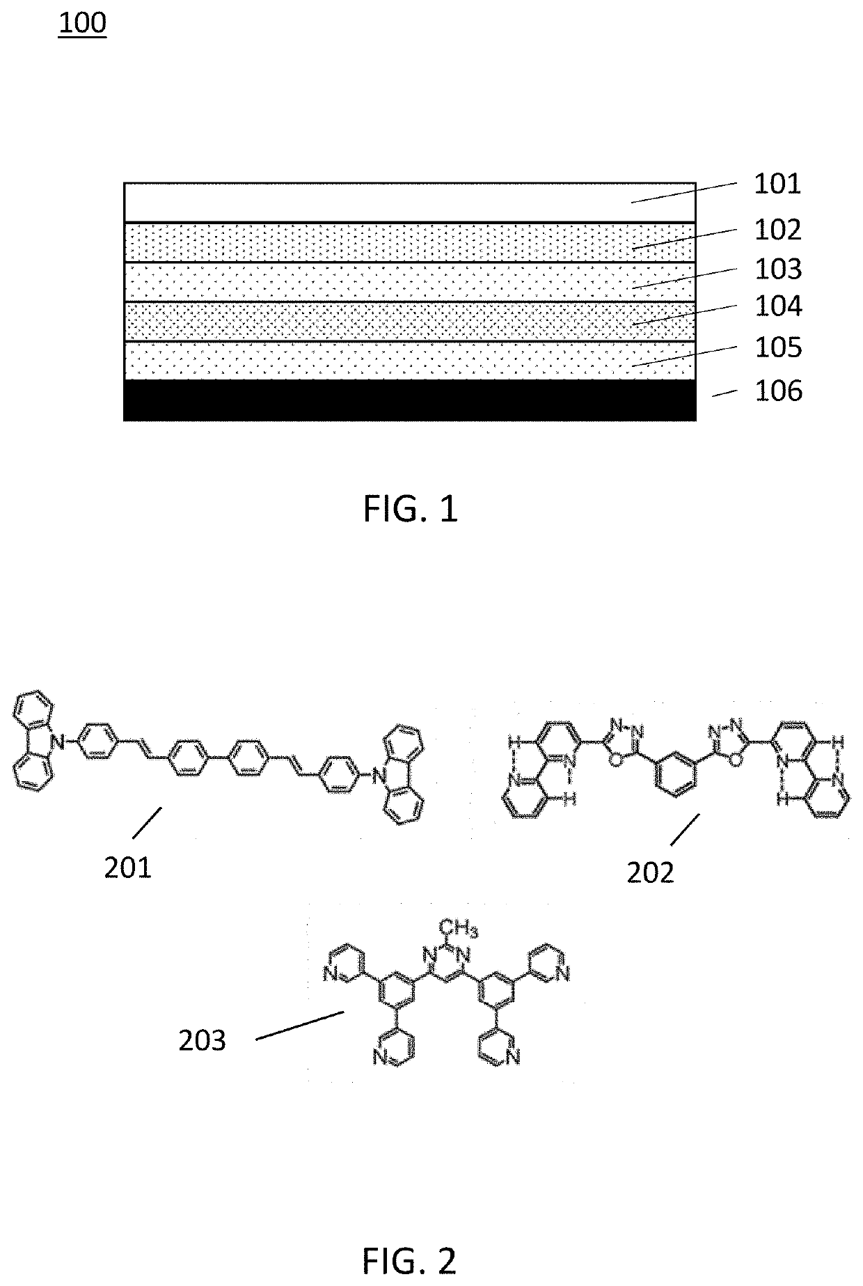
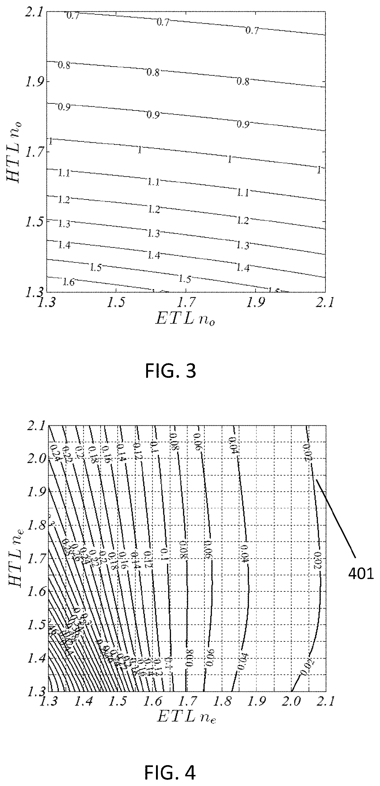
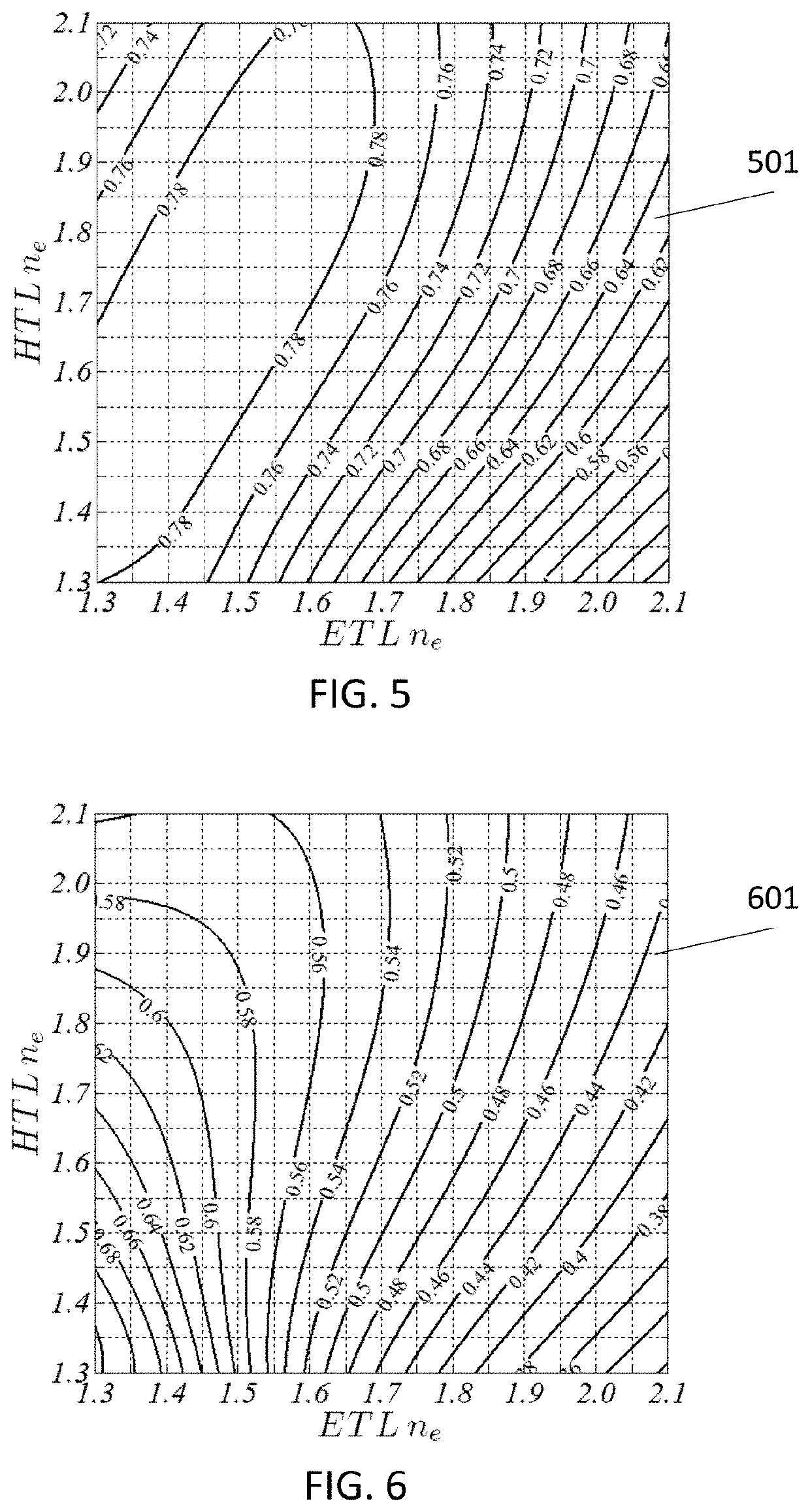
[0061]The present invention will be described with respect to particular embodiments and with reference to certain drawings but the invention is not limited thereto but only by the claims. The drawings described are only schematic and are non-limiting. In the drawings, the size of some of the elements may be exaggerated and not drawn on scale for illustrative purposes. The dimensions and the relative dimensions do not correspond to actual reductions to practice of the invention.

[0062]Furthermore, the terms first, second and the like in the description and in the claims, are used for distinguishing between similar elements and not necessarily for describing a sequence, either temporally, spatially, in ranking or in any other manner. It is to be understood that the terms so used are interchangeable under appropriate circumstances and that the embodiments of the invention described herein are capable of operation in other sequences than described or illustrated herein.

[0063]Moreover, t...


PUM

PropertyMeasurementUnit
refractive indexaaaaaaaaaa

Abstract

An organic light emitting diode comprises a hole transport layer, an emissive layer, and an electron transport layer. The hole transport layer and optionally the electron transport layer is made of a material having a refractive index having a specific anisotropy.

Description

FIELD OF THE INVENTION[0001]The invention relates to the field of light emitting devices suitable for light emitters or displays. More specifically it relates to optimization of organic light emitting diodes.BACKGROUND OF THE INVENTION[0002]Organic Light Emitting Diodes (OLEDs) are luminescent devices comprising organic layers, such as polymers. Each of these layers serves a specific purpose. In the past, a lot of effort was directed to optimization of the properties of the materials forming the structure. Several colors have been obtained, for example layers capable of producing red, green, blue, or white (which is in some OLEDs obtained by stacking three layers of the RGB materials) emission. When an appropriate combination of layers and emitters is used one can make these devices generate light with almost 100% internal efficiency. Even though light can be generated which such high efficiencies only a relatively small portion can be extracted from the structure. Due to total inte...

Claims


Application Information

Patent Timeline
Patent Type & Authority Patents(United States)
IPC IPC(8): H05B33/14H01L51/50G02F1/13363H01L51/52H01L51/44H01L51/00
CPCH01L51/5268H01L51/5012H01L51/5271H01L51/447G02F1/133634H01L51/0012H01L51/5293H01L51/442H05B33/14H01L51/5275H01L51/5203G02F2202/36H01L51/5072H01L51/5056Y02E10/549Y02P70/50H10K50/15H10K50/16H10K50/11H10K50/856H10K30/82H10K30/87H10K50/805H10K50/854H10K50/858H10K50/868H10K71/191
Inventor NEYTS, KRISTIAANCALLENS, MICHIELYOKOYAMA, DAISUKE
Owner UNIV GENT
Why Eureka
Try Eureka