Optoelectronic apparatus, a method for suppressing noise for an optoelectronic apparatus, and uses thereof

a technology of optoelectronic equipment and optoelectronic device, which is applied in the field of optoelectronic apparatus, can solve the problems of increasing the cost and size of the final product, unable to detect the low level of light level, and high noise equivalent irradiance, so as to reduce the noise equivalent irradiance or noise equivalent power, and the effect of low light level

Active Publication Date: 2020-06-09
FUNDACIO INST DE CIENCIES FOT NIQUES +1
View PDF4 Cites 0 Cited by
  • Summary
  • Abstract
  • Description
  • Claims
  • Application Information

AI Technical Summary

Benefits of technology

[0022]According to the present invention, it is preferred to use higher modulation frequencies fm because, as will be described below, 1 / f noise is the main noise to be suppressed. Therefore, the noise suppression is stronger at a higher modulation frequency.
[0029]In this sense, the heterojunction formed by the photosensitizing structure and the transport structure slows down recombination and makes it possible to collect several electric carriers for a single absorbed photon, which compounded with the high carrier mobility of the 2-dimensional material comprised in the transport structure, results in a very high photoconductive gain and responsivity.
[0065]Biosensors using chemically bonded linker molecules that enhance the selectivity for specific bio-molecules. When the molecule of interest binds to the linker, it transfer charge to the graphene or induces an electric in the graphene. This modifies the conductance of the graphene.
[0081]The applications of the present invention are in the broad photodetection field. Any photodetector based on a transport structure comprising 2D materials and a photosensitizing structure configured and arranged to absorb incident light and induce changes in the electrical conductivity of the transport structure benefits from the present invention, as they enable detection of lower light levels, reducing the noise equivalent irradiance or noise equivalent power of the detector or sensors.

Problems solved by technology

Several noise sources negatively affect the performance of that kind of apparatuses, causing a high noise equivalent irradiance or noise equivalent power thereof, which makes them unable to detect low level of light levels.
The inclusion of said external modulation components has several drawbacks, such as, among others, an increase in the cost and size of the final product, an increase in the complexity of the control needed for its operation, as more components need to be controlled, and in a synchronized manner, an increase in power consumption, more thermal and electric losses, etc.
All of said drawbacks limit the possible applications for which said optoelectronic apparatuses can be used.

Method used


Image

  • Optoelectronic apparatus, a method for suppressing noise for an optoelectronic apparatus, and uses thereof
  • Optoelectronic apparatus, a method for suppressing noise for an optoelectronic apparatus, and uses thereof
  • Optoelectronic apparatus, a method for suppressing noise for an optoelectronic apparatus, and uses thereof

Examples


embodiment 1

hutter Implemented Via Bottom Gate and Top Contact Modulation

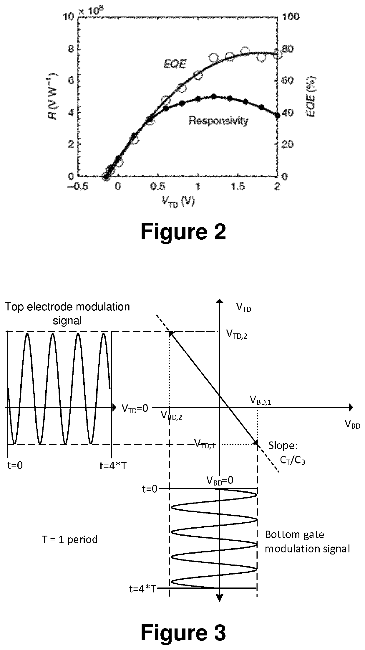
[0109]For this embodiment, the optoelectronic device of the optoelectronic apparatus of the first aspect of the present invention has the arrangement depicted by FIG. 1(a), i.e. a substrate Sb, and arranged thereon:[0110]a conductive bottom gate electrode structure Gb;[0111]a dielectric structure / layer De arranged over the conductive bottom gate electrode structure Gb;[0112]a transport structure T comprising one or more 2-dimensional layers arranged over the dielectric structure De;[0113]a photosensitizing structure / layer P (semiconducting light absorber) and arranged over the transport structure T and configured and arranged to absorb incident light and induce changes in the electrical conductivity of the transport structure T;[0114]a top electrode Et electrically connected (ohmic contact or Schottky contact) to the photosensitizing structure P; and[0115]drain D and source S electrodes electrically connected to respective...

embodiment 2

hutter Implemented Via Bottom Pate and Top Pate Modulation

[0135]For this embodiment 2, the optoelectronic device of the optoelectronic apparatus of the first aspect of the present invention has the arrangement depicted by FIG. 5, i.e. one which differs from the one of FIG. 1 in that, instead of including a top electrode, it includes a top gate Gt isolated from the photosensitizing structure P by a further dielectric structure Def.

[0136]The optoelectronic apparatus of Embodiment 2 includes the device of FIG. 5 and an electronic connection scheme as illustrated in FIG. 1(b), i.e. including voltage generators VBD, VTD, and VSD of the control unit (not shown) included in the modulation unit of the noise suppression means of the present invention, but where the voltage generator VTD is connected to the top gate Gt (instead of to a top electrode Et).

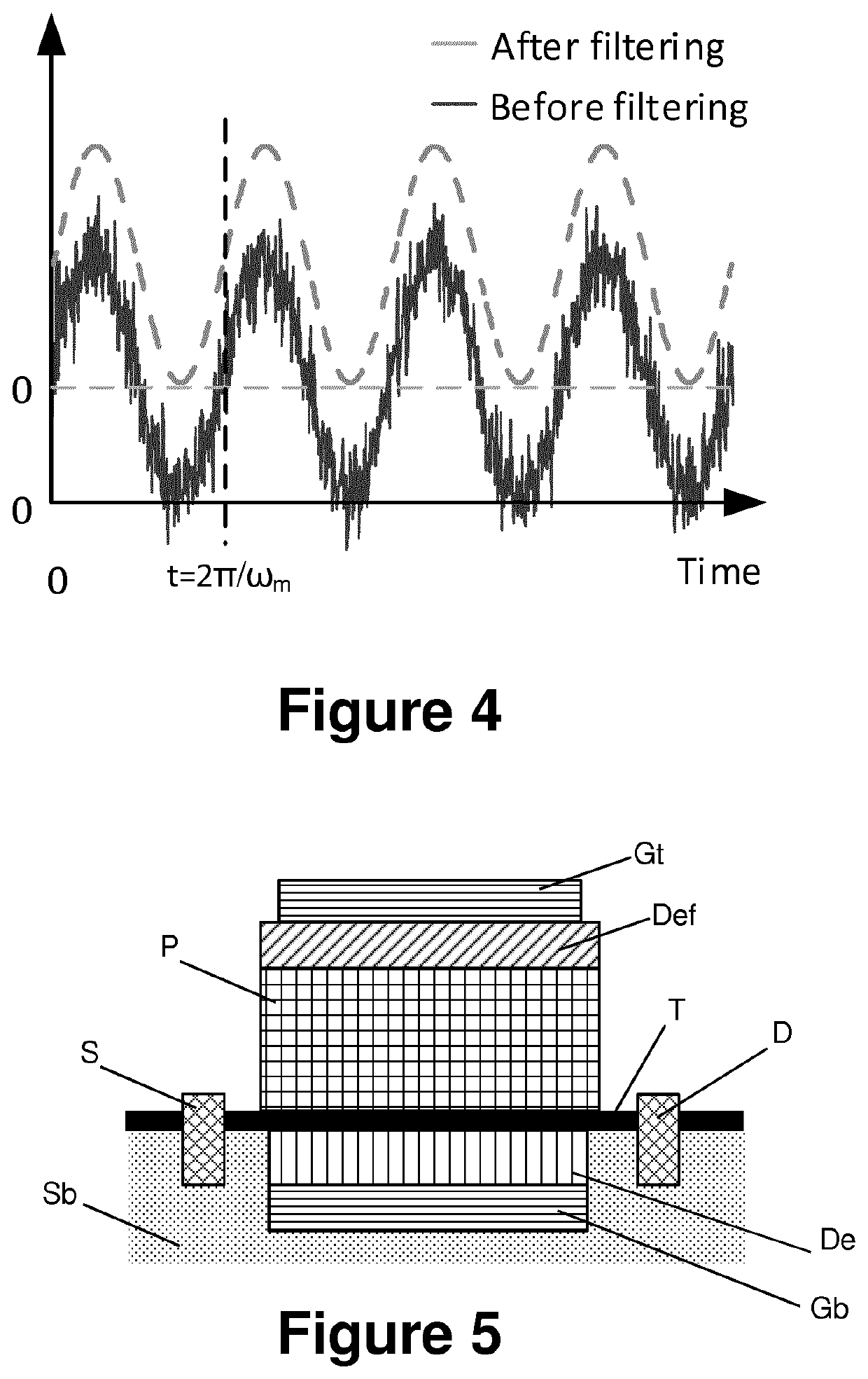
[0137]On the same grounds as described in Embodiment 1, modulation is implemented using respective oscillating signals (voltage oscillation s...

embodiment 3

ssion Using Bottom Date Modulation

[0142]For this embodiment, the optoelectronic device of the optoelectronic apparatus of the first aspect of the present invention has the arrangement depicted by FIG. 6, i.e. a substrate Sb, and arranged thereon:[0143]a conductive bottom gate electrode structure Gb;[0144]a dielectric structure / layer De arranged over the conductive bottom gate electrode structure Gb;[0145]a transport structure T comprising one or more 2-dimensional graphene layers arranged over the dielectric structure De;[0146]a photosensitizing structure / layer P (semiconducting light absorber) arranged over the transport structure T and configured and arranged to absorb incident light and induce changes in the electrical conductivity of the transport structure T; and[0147]drain D and source S electrodes electrically connected to respective separate locations of the transport structure T.

[0148]In this case, the present invention benefits specifically from the ambipolar conduction na...


PUM

PropertyMeasurementUnit
irradianceaaaaaaaaaa
quantum efficiencyaaaaaaaaaa

Abstract

The present invention relates to an optoelectronic apparatus comprising: —an optoelectronic device comprising: —a transport structure (T) comprising a 2-dimensional layer; —a photosensitizing structure (P) configured and arranged to absorb incident light and induce changes in the electrical conductivity of the transport structure (T); and —drain (D) and source (S) electrodes electrically connected to respective separate locations of the transport structure (T); —noise suppression means comprising a modulation unit including: —a control unit to generate and apply on the drain (D) or source (S) electrodes a voltage oscillating signal having a component with a frequency of ωm / 2π; and —a signal extraction unit to extract a required electric signal, from an output signal, with no components below ωm / 2π. The present invention also concerns to a method for suppressing noise for an optoelectronic apparatus according to the invention, and to the use of the apparatus as a light detector or as an image sensor.

Description

FIELD OF THE INVENTION[0001]The present invention relates, in a first aspect, to an optoelectronic apparatus, comprising noise suppression means with a modulation mechanism which operates on the optoelectronic device of the apparatus itself, doing without the use of external modulation mechanisms.[0002]A second aspect of the present invention relates to a method for suppressing noise for an optoelectronic apparatus according to the first aspect of the invention.[0003]A third aspect of the present invention concerns to the use of an optoelectronic apparatus according to the first aspect of the invention, as a light detector or as an image sensor.BACKGROUND OF THE INVENTION[0004]Optoelectronic apparatuses, such as photodetectors, which comprise the features of the preamble clause of claim 1 of the present invention are known in the art, i.e. those which comprise an optoelectronic device comprising:[0005]a transport structure comprising at least one 2-dimensional layer;[0006]a photosen...

Claims


Application Information

Patent Timeline
Patent Type & Authority Patents(United States)
IPC IPC(8): G01J1/44H04N5/357
CPCH04N5/357G01J1/44H01L27/14609H04N25/60H04N25/76
Inventor KOPPENS, FRANKGOOSSENS, STIJNKONSTANTATOS, GERASIMOS
Owner FUNDACIO INST DE CIENCIES FOT NIQUES
Why Eureka
Try Eureka