Device with light emitting element
a technology of light-emitting elements and devices, which is applied in the direction of sustainable manufacturing/processing, identification means, instruments, etc., can solve the problems of display devices and lighting devices that are likely to fail, and the shortage of organic light-emitting elements is likely to degrade, so as to prevent interfacial peeling, reduce stress, and high modulus of elasticity
- Summary
- Abstract
- Description
- Claims
- Application Information
AI Technical Summary
Benefits of technology
Problems solved by technology
Method used
Image

Examples
first embodiment
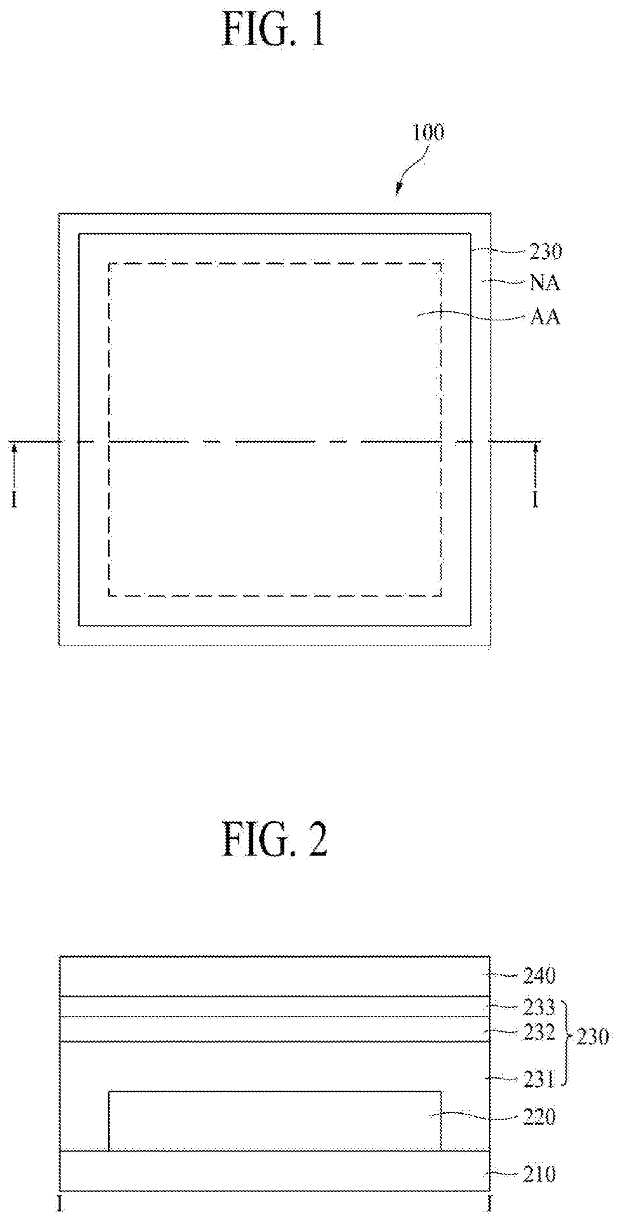
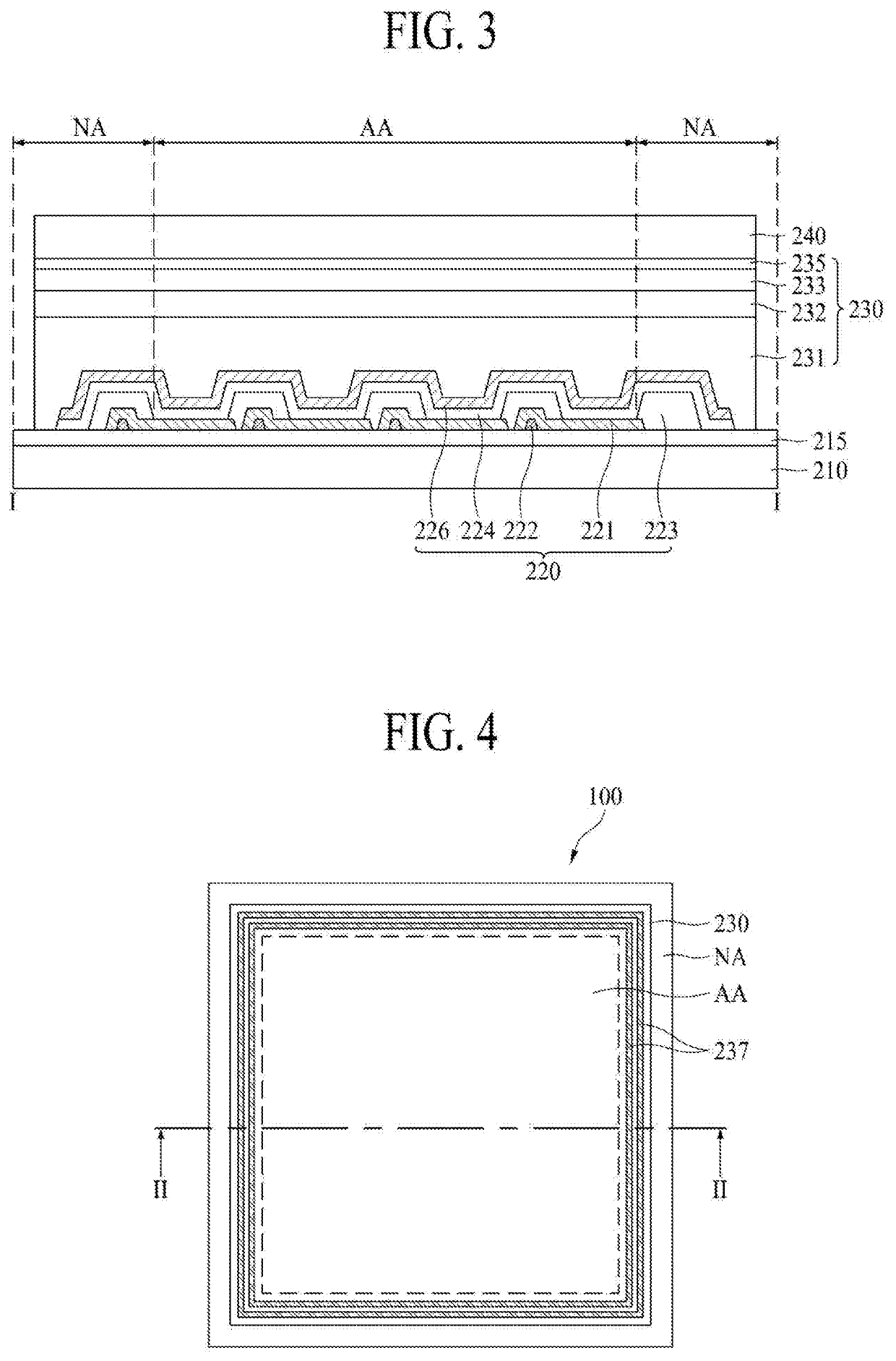
[0043]FIG. 1 is a plan view illustrating a device with light emitting elements according to a first embodiment of the present disclosure. FIG. 2 is a sectional view taken along line I-I in FIG. 1. FIG. 3 is a sectional view illustrating an example of the configuration illustrated in FIG. 2.
[0044]With reference to FIGS. 1, 2, and 3, a device 100 with light emitting elements according to a first embodiment of the present disclosure includes a first substrate 210, a light emitting element 220, an encapsulation film 230, and a second substrate 240.
[0045]In the following description, the device 100 with light emitting elements according to the first embodiment of the present disclosure is embodied as a lighting device with organic light emitting elements, but the present disclosure is not limited thereto. The device 100 with light emitting elements according to the first embodiment of the present disclosure further includes various types of light emitting elements as well as organic ligh...
second embodiment
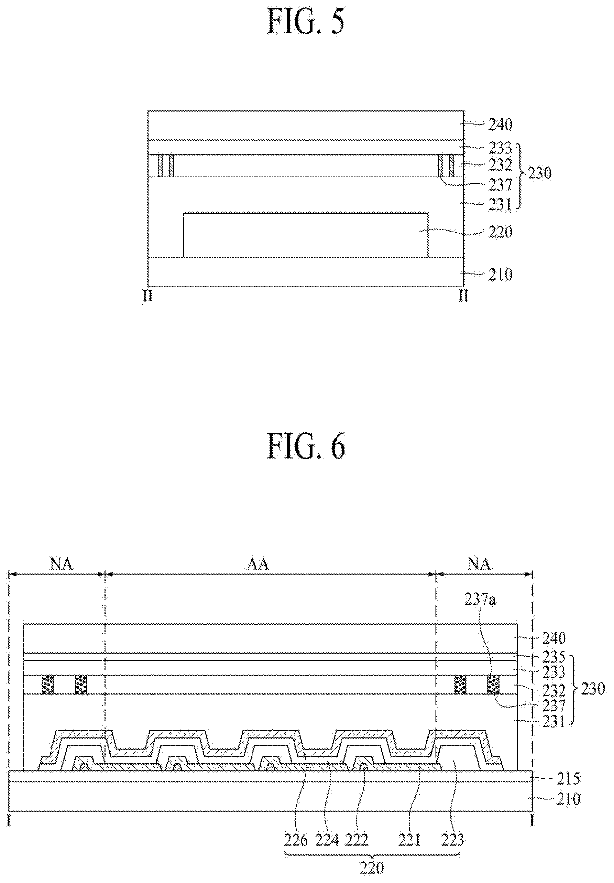
[0077]FIG. 4 is a plan view illustrating a device with light emitting elements according to a second embodiment of the present disclosure. FIG. 5 is a sectional view taken along line II-II in FIG. 4. FIG. 6 is a sectional view illustrating an example of the configuration illustrated in FIG. 5. FIG. 7 is a sectional view illustrating a modified example of the configuration illustrated in FIG. 6. FIG. 8 is a sectional view illustrating another modified example of the configuration illustrated in FIG. 6. FIG. 9 is a sectional view illustrating still another modified example.
[0078]With reference to FIGS. 4, 5, and 6, a device 100 with light emitting elements according to a second embodiment of the present disclosure includes a first substrate 210, a light emitting element 220, an encapsulation film 230, and a second substrate 240.
[0079]The first substrate 210, the light emitting element 220, and the second substrate 240 in the device 100 with light emitting elements according to the sec...
PUM
| Property | Measurement | Unit |
|---|---|---|
| modulus of elasticity | aaaaa | aaaaa |
| bending area | aaaaa | aaaaa |
| weight | aaaaa | aaaaa |
Abstract
Description
Claims
Application Information
 - R&D Engineer
- R&D Manager
- IP Professional
- Industry Leading Data Capabilities
- Powerful AI technology
- Patent DNA Extraction
Browse by: Latest US Patents, China's latest patents, Technical Efficacy Thesaurus, Application Domain, Technology Topic.
© 2024 PatSnap. All rights reserved.Legal|Privacy policy|Modern Slavery Act Transparency Statement|Sitemap