Semiconductor device

A semiconductor and sealing resin technology, applied in the direction of semiconductor devices, semiconductor/solid-state device parts, electric solid-state devices, etc., can solve the problems of product life reduction, interface peeling or cracks, etc., to achieve uniform thickness, ensure life, and high reliability Effect

Pending Publication Date: 2022-05-06
MITSUBISHI ELECTRIC CORP
View PDF1 Cites 0 Cited by
  • Summary
  • Abstract
  • Description
  • Claims
  • Application Information

AI Technical Summary

Problems solved by technology

On the other hand, in the solder reflow process, if the thickness of the solder joint is not uniform, the interface peeling or cracks may occur due to insufficient bonding strength during thermal cycles, resulting in a reduction in product life.

Method used


Image

  • Semiconductor device
  • Semiconductor device
  • Semiconductor device

Examples


Embodiment approach 1

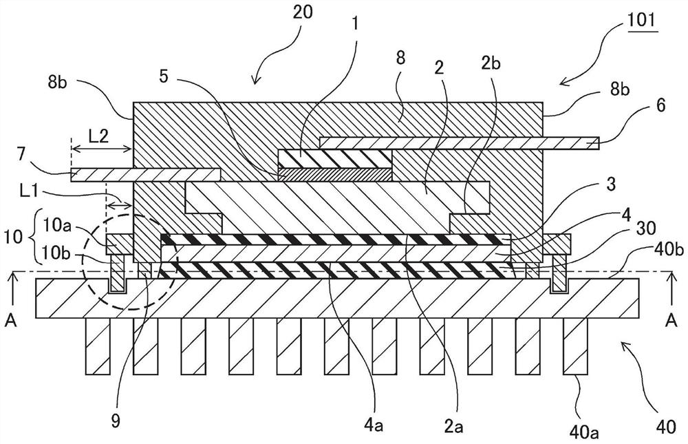
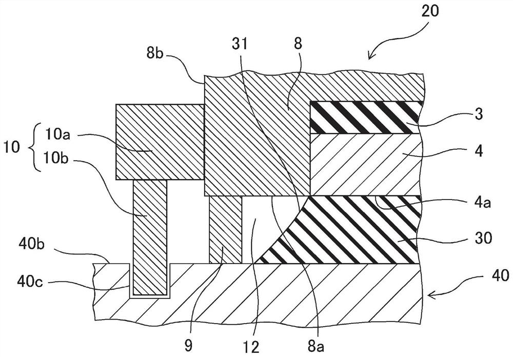
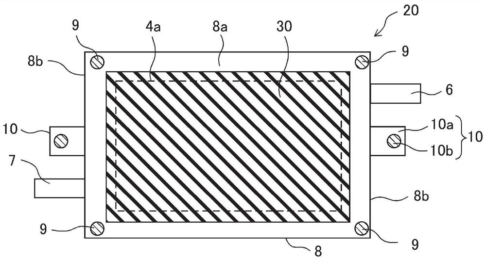
[0027] Next, the semiconductor device according to Embodiment 1 will be described based on the drawings. figure 1 is a side cross-sectional view showing a schematic configuration of the semiconductor device according to Embodiment 1, figure 2 and image 3 It is a figure explaining the thickness regulation protrusion and the positioning protrusion of the semiconductor device of Embodiment 1, figure 2 yes figure 1 A partial enlarged cross-sectional view of the part indicated by the dotted circle in , image 3 is viewed from the direction of the arrow figure 1 A cross-sectional view of the portion of the junction region indicated by A-A in . In addition, in each figure, the same code|symbol is attached|subjected to the same or a corresponding part.

[0028] The semiconductor device 101 of Embodiment 1 includes a semiconductor module 20 and a cooler 40 as basic components. The semiconductor module 20 includes: the semiconductor element 1 mounted on one surface of the metal...

Embodiment approach 2

[0075] Figure 5 is a side cross-sectional view showing a schematic configuration of a semiconductor device according to Embodiment 2, Figure 6 and Figure 7 It is a figure explaining the thickness control and positioning protrusion of the semiconductor device of Embodiment 2, Figure 6 yes Figure 5 A partial enlarged cross-sectional view of the part indicated by the dotted circle in , Figure 7 is viewed from the direction of the arrow Figure 5 Cross-sectional view of the portion of the junction region indicated by B-B in .

[0076] A semiconductor device 102 according to Embodiment 2 includes a semiconductor module 20A and a cooler 40 , and the semiconductor module 20A and the cooler 40 are bonded via solder 30 . In the semiconductor module 20A, a positioning protrusion for positioning the semiconductor module 20A and the cooler 40 is formed on the side 8b of the sealing resin 8 on which the main electrode wirings 6, 7 protrude, and the positioning protrusion also se...


PUM


Abstract

The invention provides a semiconductor device having high heat dissipation performance and reliability without enlarging the external shape of a semiconductor module. In a semiconductor device (101), a positioning protrusion (10) is formed on a side surface (8b) of a sealing resin (8) from which one end of a main electrode wiring (6, 7) protrudes. Therefore, the outer shape of the sealing resin (8) can be reduced compared with a case in which the positioning projection is formed on the bottom (8a) of the sealing resin (8). Furthermore, since the thickness-regulating protrusion (9) is provided so as to have a space (12) between the thickness-regulating protrusion (9) and the solder (30), interface peeling or cracking occurring starting from a contact portion between the thickness-regulating protrusion (9) and the solder (30) can be prevented, and the lifetime of a joint portion between the semiconductor module (20) and the cooler (40) can be ensured. Therefore, a semiconductor device (101) having high heat dissipation performance and reliability can be obtained without expanding the outer shape of the semiconductor module (20).

Description

technical field [0001] This application relates to semiconductor devices. Background technique [0002] In recent years, high output and miniaturization of semiconductor elements have been promoted, and semiconductor devices including semiconductor modules and coolers on which semiconductor elements are mounted require higher heat dissipation than conventional ones. However, heat dissipation grease widely used as a bonding material between a semiconductor module and a cooler has a low thermal conductivity, and there is concern about a decrease in heat dissipation performance due to changes over time. [0003] Therefore, by using solder having higher thermal conductivity than thermal grease as a bonding material, thermal radiation performance can be improved. On the other hand, in the solder reflow process, if the thickness of the solder joint is not uniform, the interface peeling or cracks may occur due to insufficient bonding strength during thermal cycles, resulting in a ...

Claims


Application Information

Patent Timeline
Patent Type & Authority Applications(China)
IPC IPC(8): H01L23/31H01L23/498
CPCH01L23/3121H01L23/49811H01L23/3735H01L23/4334H01L23/49562H01L23/367H01L23/3107H01L23/32H01L2924/181H01L2224/32245H01L2924/00012H01L23/433H01L23/492H01L24/73H01L24/48H01L2224/48151H01L2224/73265H01L23/49
Inventor 早柏公贵石井隆一吉井大
Owner MITSUBISHI ELECTRIC CORP
Why Eureka
Try Eureka