
OLED component and method for manufacturing the same

a manufacturing method and technology for masks, applied in the field of display, can solve the problems of many challenges in the manufacturing technology of masks, low material utilization, and difficult manufacturing of devices, and achieve the effect of simple and feasible manufacturing methods

Active Publication Date: 2020-07-28
TCL CHINA STAR OPTOELECTRONICS TECH CO LTD
View PDF11 Cites 0 Cited by
  • Summary
  • Abstract
  • Description
  • Claims
  • Application Information

AI Technical Summary

Benefits of technology

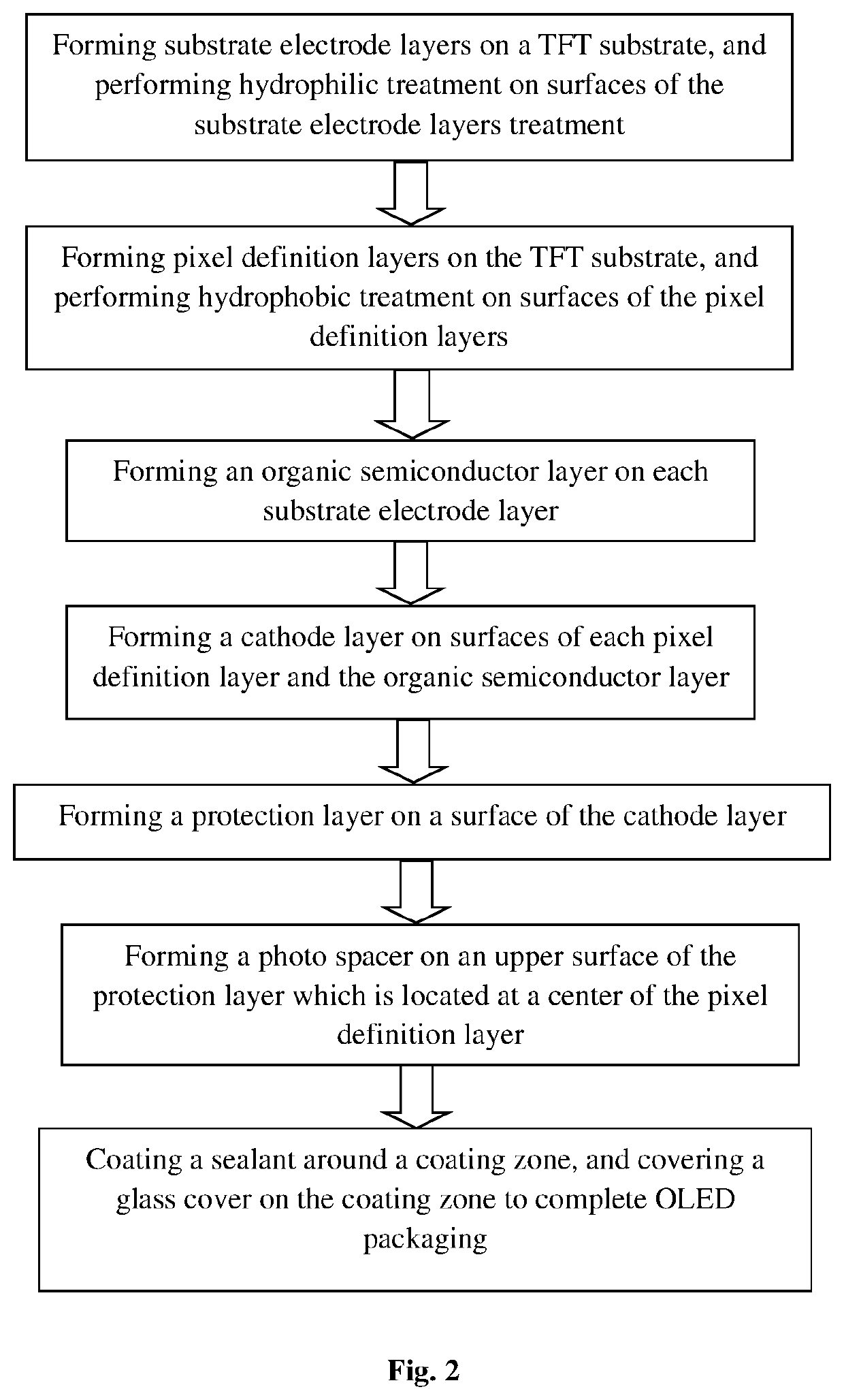
The present patent is about a new technology for making OLED displays. The technology uses ink jet printing to put a layer of material called a photo spacer on the protective layer of the OLED cathode. This method is simple and can be easily done. The technical effect of this is that it helps to improve the manufacturing process of OLED displays.

Problems solved by technology

However, in the technology, a fine mask is needed, which leads to low material utilization.
Besides, with respect to large-sized panels, there are many challenges in the manufacturing technology of the mask.
In this manner, there is a high requirement for an alignment accuracy of a device, and thus the device is difficult to be manufactured.

Method used


Image

  • OLED component and method for manufacturing the same
  • OLED component and method for manufacturing the same

Examples


Embodiment Construction

[0030]The present disclosure will be further illustrated hereinafter with reference to the drawings.

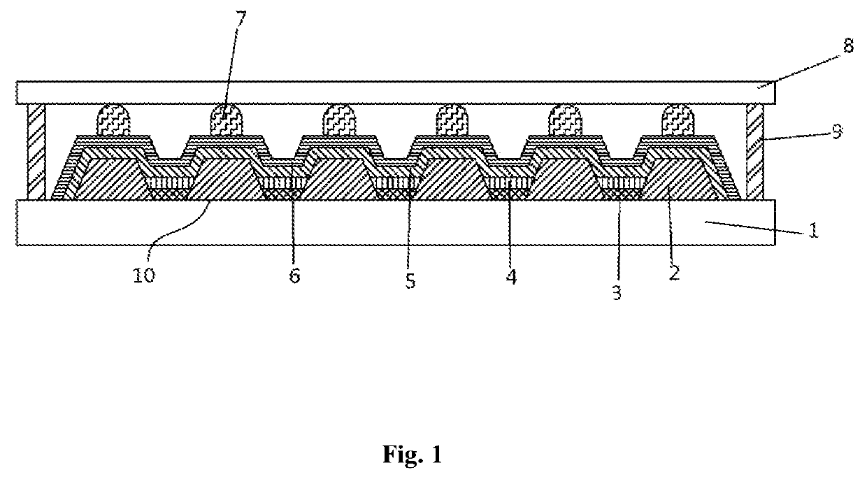
[0031]FIG. 1 schematically shows a structure of an OLED component according to the present disclosure. The OLED component comprises a TFT substrate 1, a coating zone 10, a sealant 9, a cover 8 and a photo spacer 7.

[0032]The coating zone 10 is located at a center of the TFT substrate; the sealant 9 is arranged around the coating zone 10; the cover 8 is arranged above the coating zone 10 and the sealant 9; and the photo spacer 7 is arranged on an upper surface of the coating zone 10 for supporting the cover 8. Since the photo spacer is arranged on the upper surface of the coating zone, a cell thickness uniformity of a large-sized panel can be maintained and occurrence of Newton rings can be avoided. In this manner, disadvantages in the prior art, such as high requirement for an alignment accuracy of a device and implementing difficulties thereof when the photo spacer is arranged on the ...


PUM

PropertyMeasurementUnit
widthaaaaaaaaaa
widthaaaaaaaaaa
viscosityaaaaaaaaaa

Abstract

An OLED component is disclosed, which relates to the technical field of display panel. The OLED component comprises a TFT substrate, a coating zone, a sealant, a cover and a photo spacer. The coating zone is located at a center of the TFT substrate; the sealant is arranged around the coating zone; the cover is arranged above the coating zone and the sealant; and the photo spacer is arranged on an upper surface of the coating zone for supporting the cover. Since the photo spacer is arranged on the upper surface of the coating zone, an alignment accuracy can be improved, and the OLED component can be easily manufactured. Meanwhile, a cell thickness uniformity of a large-sized panel can be maintained, and occurrence of Newton rings can be avoided.

Description

CROSS-REFERENCE TO RELATED APPLICATIONS[0001]This application claims the priority of Chinese patent application CN201710429192.1, entitled “OLED component and method for manufacturing the same” and filed on Jun. 8, 2017, the entirety of which is incorporated herein by reference.FIELD OF THE INVENTION[0002]The present disclosure relates to the technical field of display, and in particular, to an OLED component and a method for manufacturing the same.BACKGROUND OF THE INVENTION[0003]Organic light emitting diode (OLED) component has been widely used for its advantages such as good self-luminescence, high contrast, rapid response, and flexible display. A traditional OLED is made through vacuum evaporation technology. At present, mass production can be realized. However, in the technology, a fine mask is needed, which leads to low material utilization. Besides, with respect to large-sized panels, there are many challenges in the manufacturing technology of the mask. In recent years, prin...

Claims


Application Information

Patent Timeline
Patent Type & Authority Patents(United States)
IPC IPC(8): H01L51/52H01L51/56H01L51/00H01L27/32H10K99/00
CPCH01L51/56H01L51/525H01L51/0005H01L27/3246H01L2227/323H10K59/12H10K59/1201H10K71/00H10K71/135H10K59/8723H10K59/873H10K59/122H10K50/8428
Inventor LI, WENJIEWU, TSUNG YUAN
Owner TCL CHINA STAR OPTOELECTRONICS TECH CO LTD
Learn More