Bidirectional flyback converter circuit

a converter circuit and bi-directional technology, applied in the field of electric engineering, can solve the problems of complicated cooling measures, low-cost switching elements with a smaller reverse voltage, etc., and achieve the effect of improving efficiency or effect of circui

Active Publication Date: 2020-07-28
SIEMENS AG
View PDF7 Cites 2 Cited by
  • Summary
  • Abstract
  • Description
  • Claims
  • Application Information

AI Technical Summary

Benefits of technology

[0010]In view of the foregoing, it is therefore an object of the invention to provide a bidirectional flyback converter circuit, in which, in a simple and low-cost way, overvoltages or voltage loads at the switching elements caused by stray inductances can be limited and an effectiveness or an efficiency of the circuit can be improved.
[0013]The inventive bidirectional flyback converter circuit thus represents a low-cost and simple flyback converter realization for restricting voltage loads or overvoltages caused by stray inductances of the transformer at the switching elements. Energy losses through this restriction are reduced in a simple way through the use of the buck converter arranged on the input or the output side and thus the overall efficiency of the circuit or of the bidirectional flyback converter circuit is increased. The buck converter arranged on the input or the output side enables the stray energy during switching off of one of the two switching elements of the bidirectional flyback converter circuit to be reused in a very simple manner, for example, by feeding it back in on the voltage input side or on the voltage output side of the bidirectional flyback converter circuit. Furthermore, low-cost switching elements with a smaller reverse voltage can be used and complicated cooling measures can be dispensed with.
[0018]The switching element of the buck converter can be formed ideally in this case as a Metal-Oxide Semiconductor Field Effect Transistor or MOS-FET or as a bipolar transistor or as an integrated component and can be activated via an appropriate controller. A MOS-FET belongs to the field effect transistors with insulated gate, which is controlled via a control voltage (gate source voltage). When a MOS-FET is used as the switching element of the buck converter either an N-channel MOS-FET (enhancement type) or a P-channel MOS-FET (depletion type) can be used. The use of a MOS-FET represents a simple and low-cost realization of the switching elements of the buck converter, where MOS-FETs can have a relatively high switching speed.
[0020]As an alternative, it can be advantageous for the switching element of the buck converter to be realized via an integrated component. In such cases, a regulation, a driver and a switching functionality can be integrated in the integrated component and no additional activation has to be realized, as it does with the use of a MOS-FET or bipolar transistor as switching element in the buck converter.
[0021]It is useful for the primary-side and also the secondary-side switching elements of the bidirectional flyback converter as well as the switching element of the buck converter to be formed as gallium nitride based semiconductor switches. Semiconductor switches based on gallium nitride particularly allow higher switching frequencies and, when used in a switched-mode power supply, such as a flyback converter, can achieve a higher or better efficiency than usually used switching elements based on silicon for example.

Problems solved by technology

Furthermore, low-cost switching elements with a smaller reverse voltage can be used and complicated cooling measures can be dispensed with.

Method used


Image

  • Bidirectional flyback converter circuit

Examples


Embodiment Construction

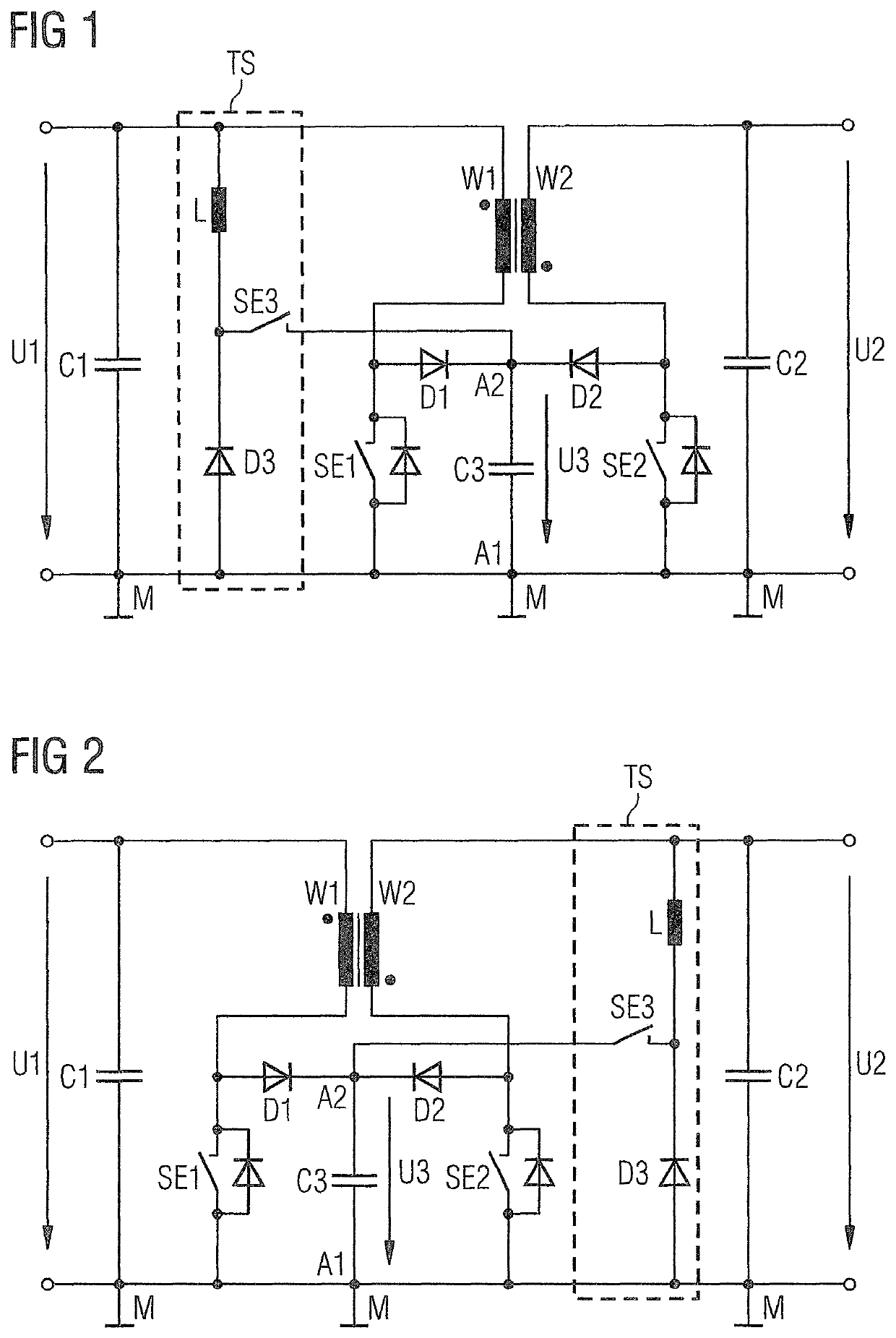
[0027]FIG. 1 shows a schematic and exemplary, bidirectional flyback converter circuit in accordance with an embodiment of the invention. The bidirectional flyback converter circuit has a transformer with a primary winding W1 and a secondary winding W2, which are inductively coupled and also wound diametrically opposed to one another. Here, the primary winding W1 is connected in this case in series with a primary-side switching element SE1 to a voltage input with an input voltage U1, where the input voltage U1 can lie in a range of 30 to 60 volts, for example. The secondary winding W2 is arranged in series with a secondary-side switching element SE2 and with a voltage output with an output voltage U2. MOS-FETs are used for the primary-side switching element SE1 and the secondary-side switching element SE2, for example. Furthermore, the primary side and secondary side or voltage input and voltage output have a common potential M, such as ground potential.

[0028]A direction of the flow ...


PUM


Abstract

A bidirectional flyback converter circuit includes a transformer with inductively coupled primary and secondary windings, primary-side and secondary-side switching elements, wherein the primary winding and secondary windings are respectively connected to a voltage input and output, where the primary-side and secondary-side switching elements are respectively arranged in series with the primary and secondary windings, where a charge capacitor is connected via a first terminal to a common potential of the primary and secondary sides, where with a second terminal, the charge capacitor is connected via a first diode to a common potential of the primary-side switching element and primary winding and via a second diode to a common potential of the secondary-side switching element and secondary winding, and where a buck converter is arranged on the input or output side, through which a voltage present at the charge capacitor can be regulated to a predeterminable value.

Description

BACKGROUND OF THE INVENTION1. Field of the Invention[0001]The present invention relates in general to the field of electrical engineering, in particular to the area of power electronics and also power electronics circuits. Specifically the present invention relates to a bidirectional flyback converter circuit, which comprises a transformer with inductively coupled primary and secondary windings, a primary-side switching element and a secondary-side switching element, where the primary winding is connected to a voltage input of the flyback converter circuit and the primary-side switching element is arranged in series with the primary winding, and where the secondary winding is connected to a voltage output of the flyback converter circuit and the secondary-side switching element is arranged in series with the secondary winding.2. Description of the Related Art[0002]What is known as a flyback converter represents a version of a switched-mode power supply, with which electrical loads c...

Claims


Application Information

Patent Timeline
Patent Type & Authority Patents(United States)
IPC IPC(8): H02M3/335H02M1/34
CPCH02M3/33584H02M3/335H02M2001/342Y02B70/10H02M1/342
Inventor PORTISCH, DANIEL
Owner SIEMENS AG
Why Eureka
Try Eureka