
Magnetic structure based on synthetic antiferromagnetic free layer and derivative SOT-MRAM

a technology of free layer and sot-mram, which is applied in the field of magnetic structure based on synthetic antiferromagnetic free layer and derivative sot-mram, can solve the problem of limiting the density of mram cells in memory arrays, and achieve the effects of reducing the volume of the device, increasing the density of mram cells, and reducing the thickness of the magnetic tunnel junction

Active Publication Date: 2020-08-04
XI AN JIAOTONG UNIV
View PDF4 Cites 2 Cited by
  • Summary
  • Abstract
  • Description
  • Claims
  • Application Information

AI Technical Summary

Benefits of technology

[0006]An object of the present invention is to provide a magnetic structure comprising a magnetic tunnel junction which comprises a free layer based on a synthetic antiferromagnetic multilayer structure and a spin-orbit layer, wherein the magnetic structure is applied to a SOT-MRAM (Spin-orbit Torque Magnetic Random Access Memory) with a lower density of a write current, so as to reduce a density of the write current, improve a density of MRAM cells in a memory array and achieve ultralow power consumption of the memory cell.
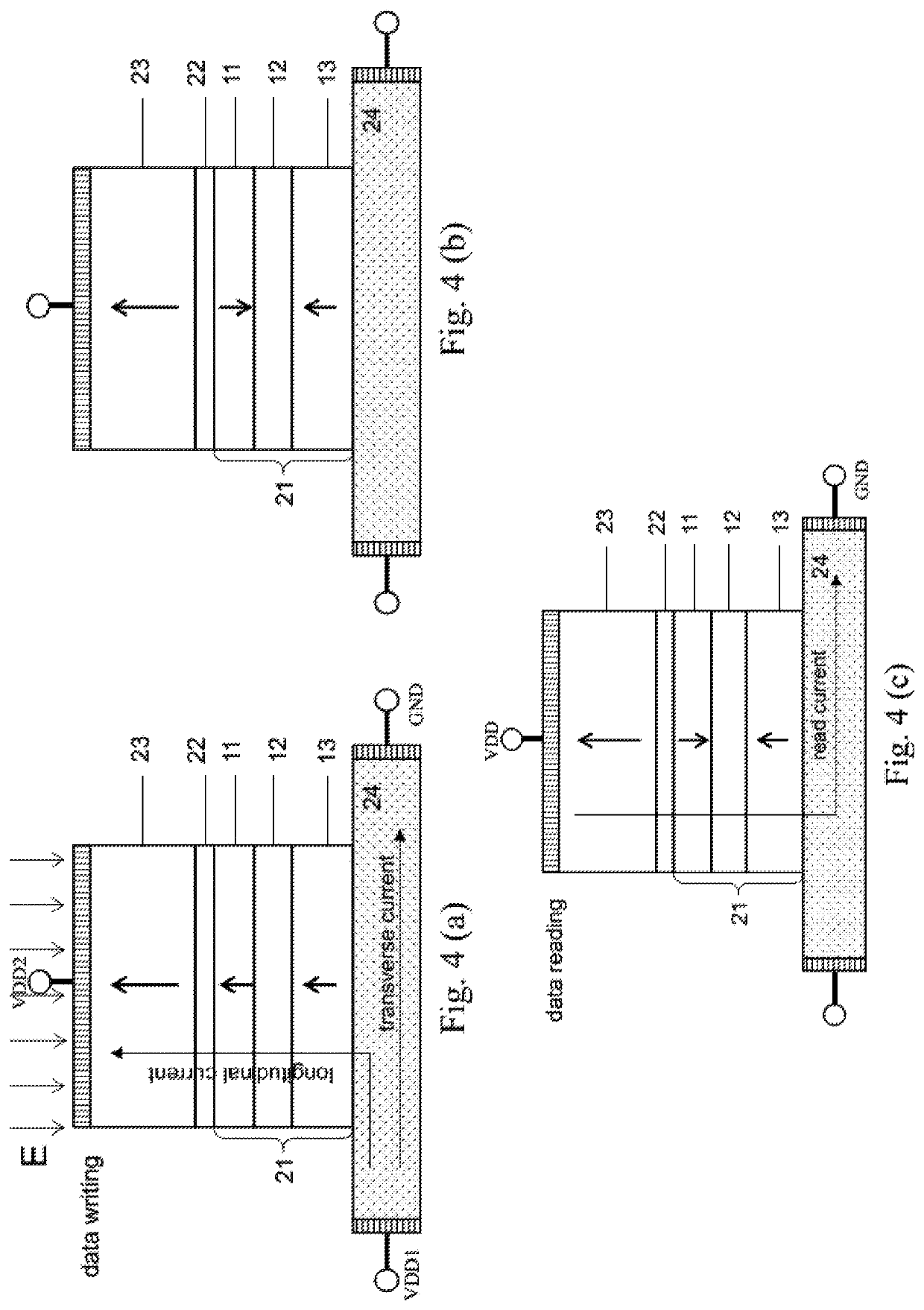
[0007]Another object of the present invention is to provide a SOT-MRAM (Spin-orbit Torque Magnetic Random Access Memory) based on a synthetic antiferromagnetic multilayer structure which acts as a free layer of the magnetic tunnel junction for assisting data writing by an electric field, thereby achieving ultrahigh speed of switching.
[0008]Another object of the present invention is to provide a write method of a read and write separated SOT-MRAM, which greatly reduces the impact of current density on the working life of MRAM, in order to achieve high endurance of a SOT-MRAM.
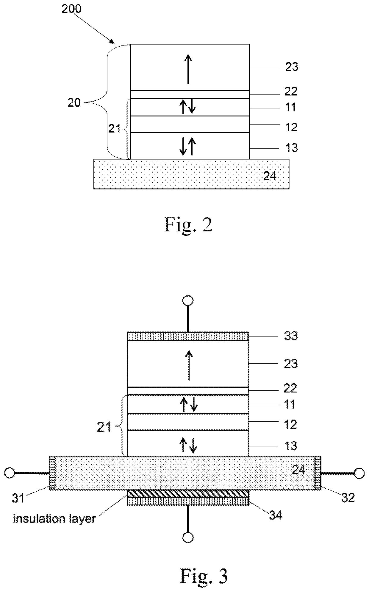
[0051]Compared with the prior art, the present invention has characteristics as follows. (1) Contrast to STT-MRAM (Spin-transfer Torque Magnetic Random Access Memory), the present invention has a lower critical switching density approximate in a range of 1×10² to 1×10⁷ A / cm2 while the magnetization flip critical switching current density of the STT-MRAM is about 1×10⁷ A / cm2. (2) The transformation between the antiferromagnetic coupling and the ferromagnetic coupling of the synthetic antiferromagnetic multilayer structure is regulated by the electric field, so that the volume of the device is reduced significantly by reducing the thickness of the magnetic tunnel junction, so as to increase the density of MRAM cells in a memory array. (3) The structure of read-write separation helps to protect the magnetic structure from being damaged by high current density during frequent rewriting operations.

Problems solved by technology

However, the density of the critical switching current of current SOT-MRAMs is still high, which limits the density of MRAM cells in a memory array.

Method used


Image

  • Magnetic structure based on synthetic antiferromagnetic free layer and derivative SOT-MRAM
  • Magnetic structure based on synthetic antiferromagnetic free layer and derivative SOT-MRAM
  • Magnetic structure based on synthetic antiferromagnetic free layer and derivative SOT-MRAM

Examples


Embodiment Construction

[0062]The technical solution of the present invention is described in detail with accompanying drawings and embodiments as follows, the following embodiments relate to a magnetic random access memory which is capable of controlling a synthetic antiferromagnetic multilayer structure to transform from an antiferromagnetic coupling to a ferromagnetic coupling by an electric field, but do not constitute a basis for any limitation of the present invention.

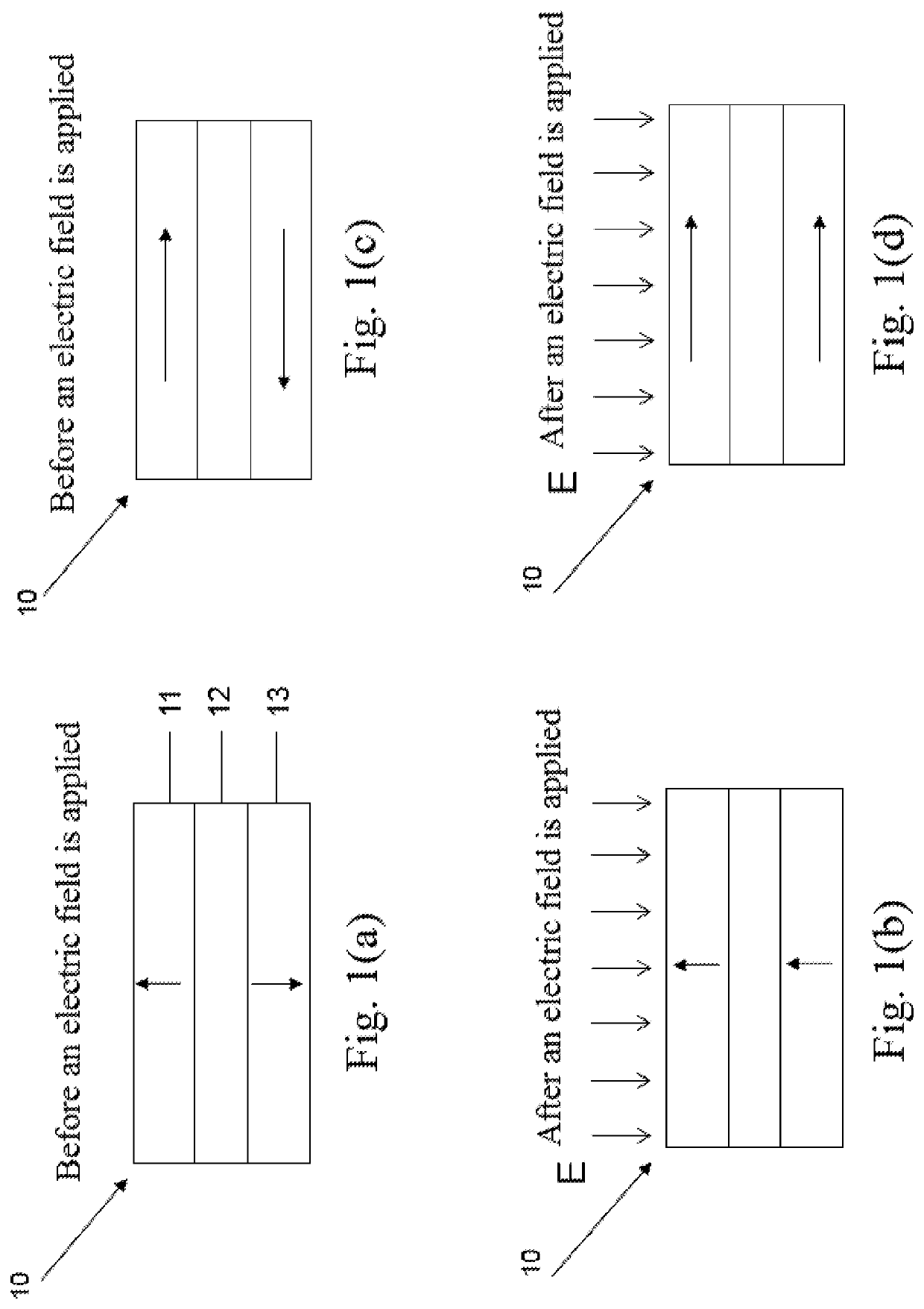
[0063]FIGS. 1(a)-(d) show a synthetic antiferromagnetic multilayer structure 10 which is able to be regulated by an electric field according to a preferred embodiment of the present invention. FIGS. 1(a)-(d) and any other drawings of the present invention are not drawn to scale. FIGS. 1(a)-(b) show a synthetic antiferromagnetic multilayer structure 10 with a magnetization direction approximately pointing vertically out of a wafer surface, FIGS. 1(c)-(d) show a synthetic antiferromagnetic multilayer structure 10 with a magnetization dire...


PUM

PropertyMeasurementUnit
diameteraaaaaaaaaa
thicknessaaaaaaaaaa
magnetic structureaaaaaaaaaa

Abstract

A magnetic structure includes a magnetic tunnel junction based on a synthetic antiferromagnetic free layer which is regulated by an electric field, and a spin-orbit layer located below the magnetic tunnel junction. The transformation from the antiferromagnetic coupling to the ferromagnetic coupling of the free layer based on a synthetic antiferromagnetic multilayer structure is controlled by an electric field. A spin-orbit torque magnetic random access memory, which includes the magnetic structure, is able to realize stable data writing under the combined interaction of electric field and current, and has advantages of simple structure for scaling, ultralow power consumption, ultrahigh speed of switching, radiation resistance and non-volatility.

Description

CROSS REFERENCE OF RELATED APPLICATION[0001]The present invention claims priority under 35 U.S.C. 119(a-d) to CN 201811088726.X, filed Sep. 18, 2018.BACKGROUND OF THE PRESENT INVENTIONField of Invention[0002]The present invention relates to the circuits and devices having magnetic or ferromagnetic materials or structures and the applications thereof, and more particularly to a free layer based on a synthetic antiferromagnetic multilayer structure which is regulated by an electric field and a SOT-MRAM (Spin-orbit Torque Magnetic Random Access Memory) using a spin-orbit torque for data erasing.Description of Related Arts[0003]The MTJ (magnetic tunnel junction) comprises two magnetic metal layers and an ultra-thin insulation layer sandwiched between the two magnetic metal layers. If a bias voltage is applied between the two magnetic metal layers, the insulation layer is very thin, so electrons are able to pass through the potential barrier by the tunneling effect. Under a given bias vo...

Claims


Application Information

Patent Timeline
Patent Type & Authority Patents(United States)
IPC IPC(8): G11C11/16H01F10/32H01L27/22H01L43/02H01L43/10
CPCG11C11/161G11C11/1673G11C11/1675H01F10/325H01F10/329H01F10/3259H01F10/3272H01L27/222H01L43/02H01L43/10G11C11/18G11C11/1693H01F10/1936H10B61/00H10N50/10H10N50/85H10N50/80
Inventor MIN, TAIZHOU, XUEZHOU, XUESONGWANG, LEI
Owner XI AN JIAOTONG UNIV
Learn More