Semiconductor device having first and second switching regions respectively controlled by first and second control signals output by a controller

a technology of switching region and control signal, which is applied in the direction of electronic switching, pulse technique, power conversion system, etc., can solve the problems of increasing turn-on loss and insufficient consideration of turn-on loss

Active Publication Date: 2020-09-08
MITSUBISHI ELECTRIC CORP
View PDF12 Cites 5 Cited by
  • Summary
  • Abstract
  • Description
  • Claims
  • Application Information

AI Technical Summary

Benefits of technology

[0006]The present invention has been devised in order to solve the problems described above, and an object of the present invention is to provide a semiconductor device capable of adjusting controllability and a turn-on loss during turn-on by enabling adjustment of a time change rate (dv / dt) of a voltage applied to both ends of a semiconductor chip.
[0008]The semiconductor device according to the present invention makes it possible to adjust a time change rate (dv / dt) of the voltage applied to both ends of the semiconductor chip during turn-on by the control signal outputted from the control unit. Therefore, a semiconductor device capable of adjusting controllability and a turn-on loss during turn-on can be provided.

Problems solved by technology

However, in the semiconductor device described in WO 2014 / 038064, a loss that occurs during the turn-on, that is, a turn-on loss is not sufficiently considered.
That is, the time change rate (dv / dt) of the voltage applied to both the ends of the semiconductor chip during the turn-on needs to be adjusted because the controllability is deteriorated when the time change rate (dv / dt) is too large and the turn-on loss increases when the time change rate (dv / dt) is too small.

Method used


Image

  • Semiconductor device having first and second switching regions respectively controlled by first and second control signals output by a controller
  • Semiconductor device having first and second switching regions respectively controlled by first and second control signals output by a controller
  • Semiconductor device having first and second switching regions respectively controlled by first and second control signals output by a controller

Examples


first embodiment

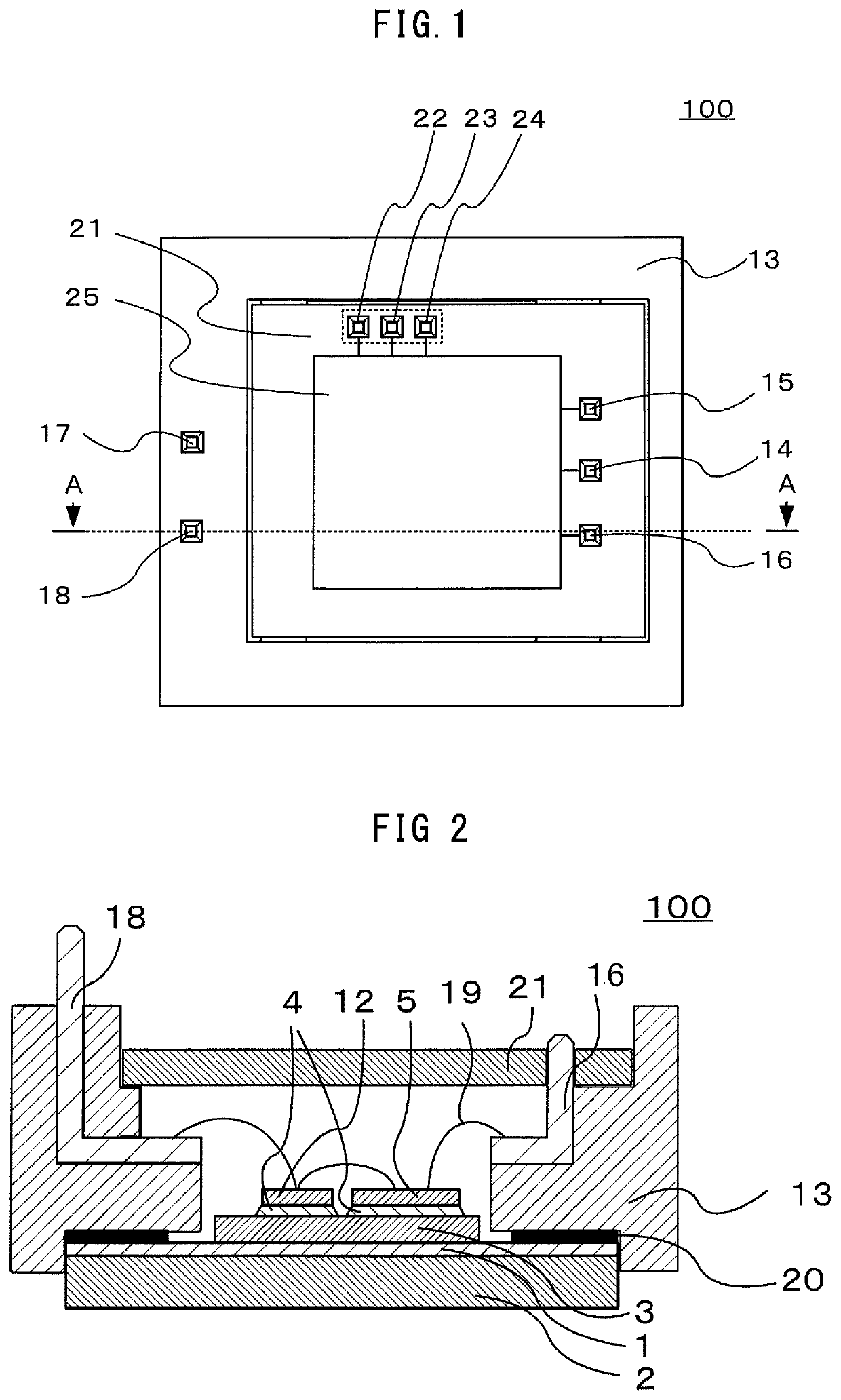
[0020]The configuration of a semiconductor device 100 according to a first embodiment of the present invention is explained. FIG. 1 is a plan view showing the configuration of the semiconductor device according to the first embodiment of the present invention. FIG. 2 is a sectional view showing the configuration of the semiconductor device according to the first embodiment. FIG. 1 is a plan view showing the semiconductor device 100 viewed from above. FIG. 2 is a sectional view taken along an A-A line shown in FIG. 1. In FIGS. 1 and 2, several members such as a sealing material filled on the inside of the semiconductor device 100 and a lid provided on the upper surface of the semiconductor device 100 according to necessity are omitted.

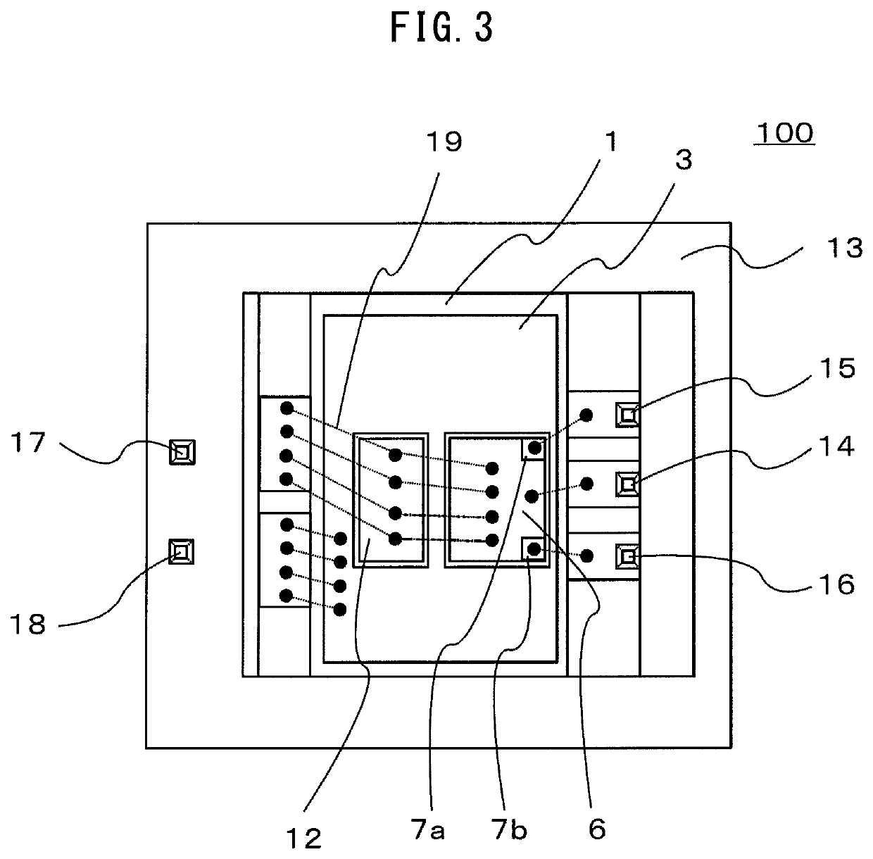
[0021]In FIG. 1, the semiconductor device 100 includes a resin case 13 having a rectangular shape in plan view and includes a control board 21 on the inner side of the resin case 13. The control board 21 includes a control section 25 and a plurality of ...

second embodiment

[0055]The configuration of a semiconductor device 200 according to a second embodiment of the present invention is explained. In the above explanation of the first embodiment, the second predetermined period t2 is controlled in the preset period by the configuration of the control section 25. However, in the second embodiment, the semiconductor device 200 includes a voltage detection circuit 250 for controlling the second predetermined period t2, and the second predetermined period t2 is controlled on the basis of a voltage between a high-potential-side signal terminal 260 and the reference-potential signal terminal 14 detected by the voltage detection circuit 250. In the second embodiment of the present invention, explanation about portions same as or corresponding to the portions in the first embodiment of the present invention is omitted.

[0056]The configuration of the semiconductor device 200 according to the second embodiment of the present invention is explained with reference ...

third embodiment

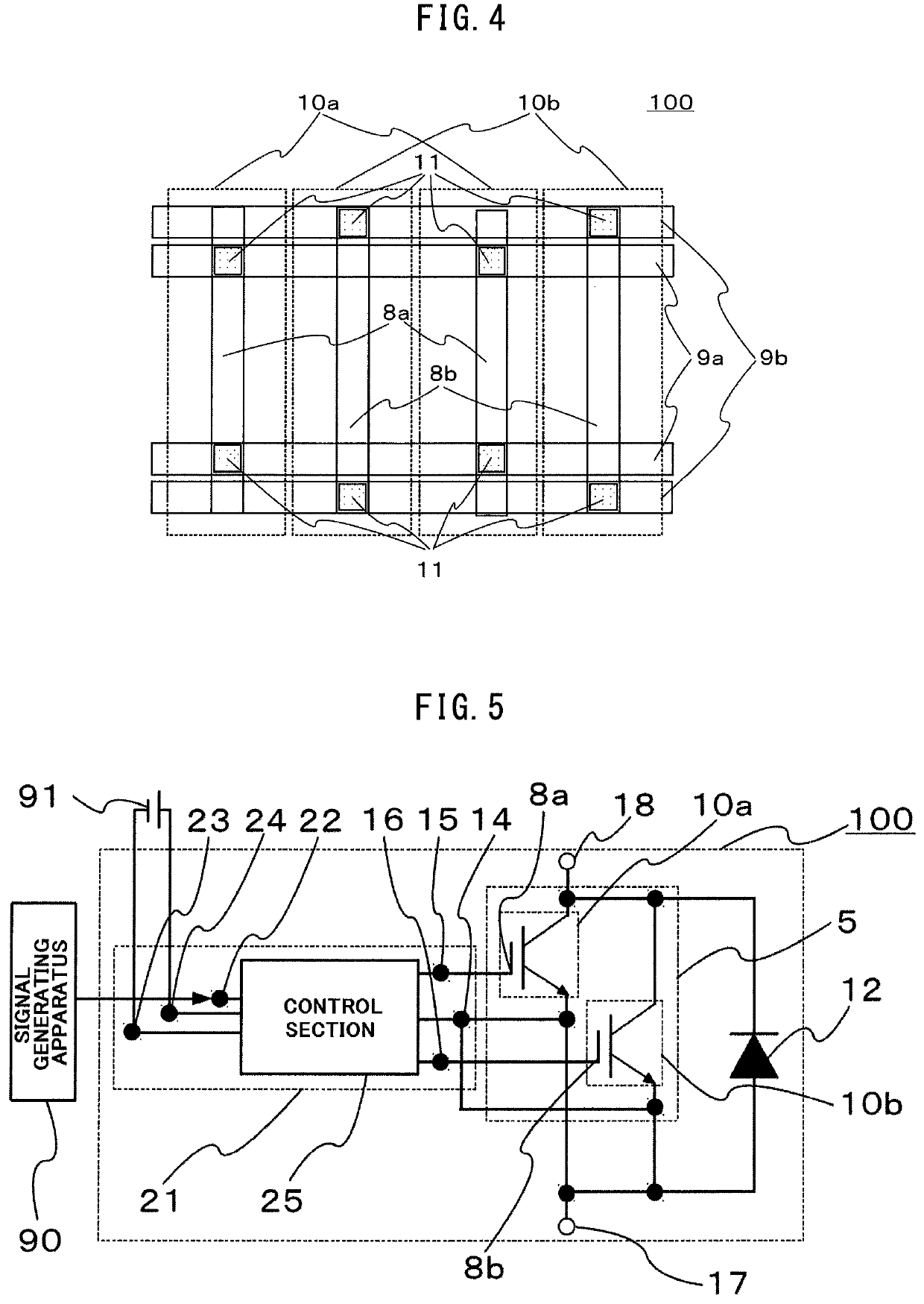
[0064]FIG. 10 is a plan view showing the configuration of a driving wire of a semiconductor chip mounted on a semiconductor device according to a third embodiment of the present invention. A semiconductor device 300 according to the third embodiment of the present invention is configured such that an electric charge amount necessary for completion of a voltage rise of second gate electrodes 308b is larger than an electric charge amount necessary for completion of a voltage rise of first gate electrodes 308a. The electric charge amounts necessary for the voltage rise completion of the first gate electrodes 8a and the second gate electrodes 8b indicate electric charge amounts necessary for the first gate electrodes 308a and the second gate electrodes 308b until the first gate electrodes 308a and the second gate electrodes 308b have a voltage equivalent to a set voltage of the power supply 91. The semiconductor device 300 in the third embodiment of the present invention is the same as ...


PUM

PropertyMeasurementUnit
thresholdaaaaaaaaaa
channel currentaaaaaaaaaa
electric chargeaaaaaaaaaa

Abstract

First and second switching regions include first and second gate electrodes respectively. Channel currents of the first and second switching regions are controlled according to electric charge amounts supplied by control signals input to the first and second gate electrodes respectively. The second switching region is connected in parallel with the first switching region. A control section outputs a first control signal for turning-on the first switching region to the first gate electrode and a second control signal for turning-on the second switching region to the second gate electrode. The control section stops outputting the second control signal after a first predetermined period elapses from a start of outputting the first and second control signals, and outputs the second control signal after a second predetermined period elapses from a stop of outputting the second control signal.

Description

BACKGROUND OF THE INVENTIONField[0001]The present invention relates to a semiconductor device.Background[0002]For a semiconductor device mounted with an insulated gate bipolar transistor (IGBT) or a metal oxide semiconductor field effect transistor (MOSFET), which is a semiconductor chip including gate electrodes, there is a demand for a technique to reduce a time change rate (dv / dt) of a voltage applied to both ends of the semiconductor chip when switching from an OFF state to an ON state is performed, that is, during so-called turn-on.[0003]WO 2014 / 038064 describes a semiconductor device that shifts timing of turn-on of a driving signal supplied to a first gate electrode and timing of turn-on of a driving signal supplied to a second gate electrode by a predetermined time during the turn-on in order to reduce a time change rate (dv / dt) of an output voltage during the turn-on and improve controllability.SUMMARY[0004]However, in the semiconductor device described in WO 2014 / 038064, a...

Claims


Application Information

Patent Timeline
Patent Type & Authority Patents(United States)
IPC IPC(8): H03K17/687H01L25/18H03K17/567H01L25/16H01L25/07
CPCH01L25/18H01L25/16H03K17/6871H03K17/567H01L25/072H03K17/161H03K17/165H03K17/687H03K2017/6878H01L2224/48137H01L2224/48157H01L2224/4816H01L2224/49109H01L2224/49111H01L2224/49175H01L2224/49112H01L2224/49171H01L2224/49177H01L2224/32227H01L2224/73265H01L25/162H02M1/088H01L2224/291H01L2924/00014H01L2924/19107H01L2224/0603H01L2924/014H01L2224/45099
Inventor EGUCHI, KEISUKEINOUE, TAKAHIROYONEYAMA, REIUOTA, SHIORIMURAKAMI, HARUHIKO
Owner MITSUBISHI ELECTRIC CORP
Why Eureka
Try Eureka