PCB stencil manufacturing method and system

a manufacturing method and stencil technology, applied in the field of electronic manufacturing, can solve the problems of easy to miss the opening, easy to be damaged, and difficult to achieve the effect of saving more than 60% to 80% of the time, maximizing the use of design data cad and gerber, and greatly reducing manual intervention

Active Publication Date: 2020-11-03
VAYO SHANGHAI TECH
View PDF36 Cites 0 Cited by
  • Summary
  • Abstract
  • Description
  • Claims
  • Application Information

AI Technical Summary

Benefits of technology

[0032]As described above, the PCB stencil manufacturing method and system consistent with the present invention have the following beneficial effects: Usage of design data CAD and Gerber may be maximized. That is, the design data CAD and Gerber are accurately utilized for 100%, and accuracy reaches 100%. In addition, manual intervention is greatly reduced, and the PCB stencil manufacturing may be completed by using several simple steps, thereby saving more than 60% to 80% of the time. Knowledge requirements of an apparatus operator are not high, and a common operator can complete the PCB stencil manufacturing. The present invention changes the conventional working manner and implements automatic or semi-automatic generation of a solder pad element opening pattern during PCB stencil manufacturing. Not only manpower is greatly saved and the efficiency of stencil manufacturing is improved, but also accuracy of stencil manufacturing is improved, thereby the present invention has a relatively large advantage.

Problems solved by technology

This manner makes it particularly easy to miss the opening, and consequently, after a stencil arrives at a factory, whether an opening of the stencil is correct or missed often needs to be manually checked through naked eyes.
Not only the method is extremely complex, but also an opening is easily missed.
In addition, the introduced Gerber file must be correct; otherwise an error on the Gerber file can only be found when an actual PCB is compared at last, such as missing a solder pad.
In view of this, how to find a solution that can complete the stencil manufacturing more rapidly and efficiently has become an urgent problem to be resolved by those skilled in the art.

Method used


Image

  • PCB stencil manufacturing method and system
  • PCB stencil manufacturing method and system

Examples


Embodiment Construction

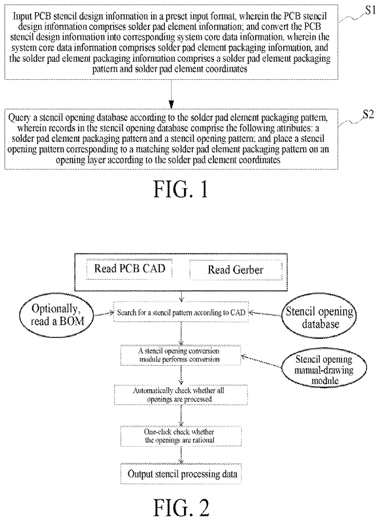
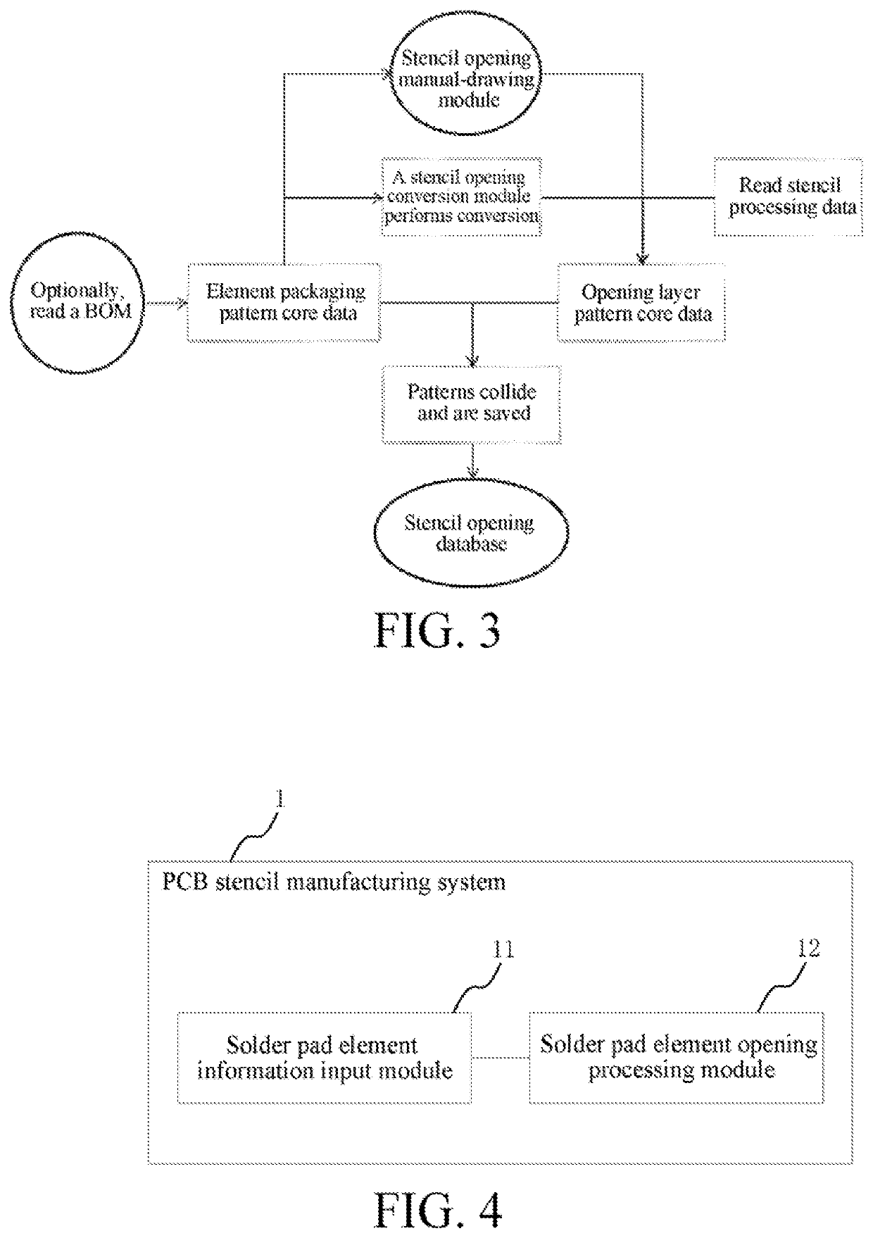
[0041]Implementations of the present invention are described in the following by using specific embodiments. Those skilled in the art can easily understand other advantages and effects of the present invention through contents disclosed in this specification. The present invention may alternatively be implemented or applied by using other different specific implementations. Various details in this specification may also be modified or changed based on a different idea or application without departing from the spirit of the present invention.

[0042]It should be noted that, figures provided in the present embodiments merely describe a basic concept of the present invention in a schematic manner, and therefore, the figures only show components related to the present invention, and are not drawn according to the numbers, shapes, and sizes of the components in an actual implementation. In an actual implementation, the shapes, numbers, and scales of the components may be a random change, a...


PUM


Abstract

A PCB stencil manufacturing method and system. The method comprises: inputting PCB stencil design information in a preset input format, the PCB stencil design information comprises solder pad element information; and converting the PCB stencil design information into corresponding system core data information, the system core data information comprises solder pad element packaging information, and the solder pad element packaging information comprises a solder pad element packaging pattern and solder pad element coordinates; and querying a stencil opening database according to the solder pad element packaging pattern, records in the stencil opening database comprise the following attributes: a solder pad element packaging pattern and a stencil opening pattern; and placing a stencil opening pattern corresponding to a matching solder pad element packaging pattern to an opening layer according to the solder pad element coordinates.

Description

CROSS REFERENCE TO RELATED PATENT APPLICATION[0001]The present application is the US national stage of PCT / CN2016 / 099799 filed on Sep. 23, 2016, which claims the priority of the Chinese patent application No. CN2016105939725 filed on Jul. 26, 2016, which application is incorporated herein by reference.BACKGROUND OF THE PRESENT INVENTIONField of Invention[0002]The present invention relates to the technical field of electronic manufacturing, and in particular, to a PCB stencil manufacturing method and system.Description of Related Arts[0003]In the electronic manufacturing industry, stencils are basically manufactured by using a Gerber file, and are mostly manually manufactured. This manner makes it particularly easy to miss the opening, and consequently, after a stencil arrives at a factory, whether an opening of the stencil is correct or missed often needs to be manually checked through naked eyes. A traditionally preferred manufacturing manner generally includes the following steps:...

Claims


Application Information

Patent Timeline
Patent Type & Authority Patents(United States)
IPC IPC(8): G06F30/392G06F16/903G05B19/4099G06F30/39G06F30/36H05K3/00H05K3/12G06F113/18
CPCG06F30/39G06F30/36G05B19/4099G06F16/90335G06F30/392H05K3/1225H05K3/0005G06F2113/18
Inventor QIAN, SHENGJIELIU, FENGSHOULIU, JIUXUANLIU, JISHUO
Owner VAYO SHANGHAI TECH
Why Eureka
Try Eureka