Component having enhanced efficiency and method for production thereof

a technology of components and efficiency, applied in the field of components, can solve problems such as efficiency loss of optoelectronic components, and achieve the effect of increasing efficiency

Active Publication Date: 2020-12-08
OSRAM OLED
View PDF52 Cites 0 Cited by
  • Summary
  • Abstract
  • Description
  • Claims
  • Application Information

AI Technical Summary

Benefits of technology

[0004]Embodiments provide a component having increased efficiency. Embodiments further provide an efficient method for producing a component.
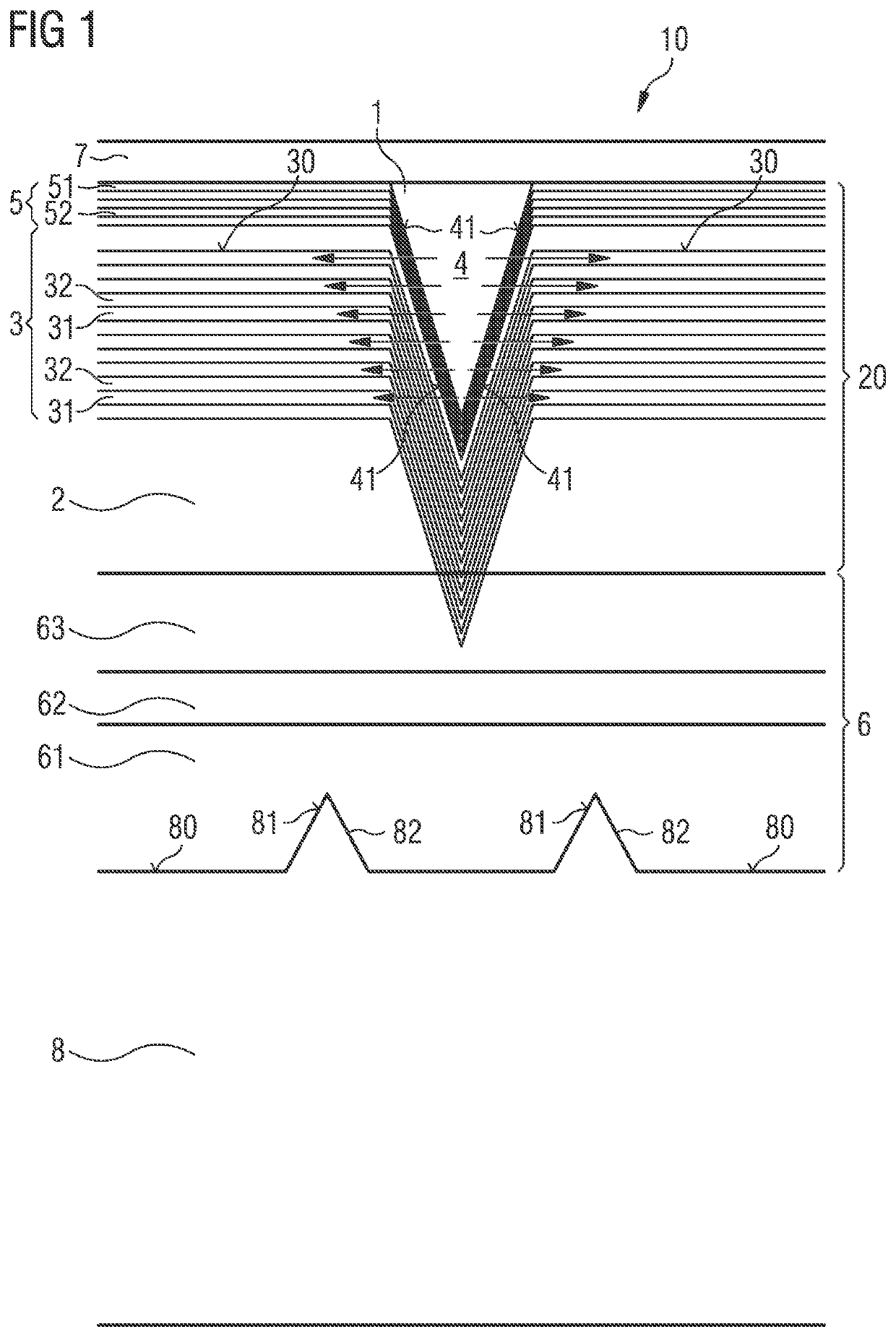
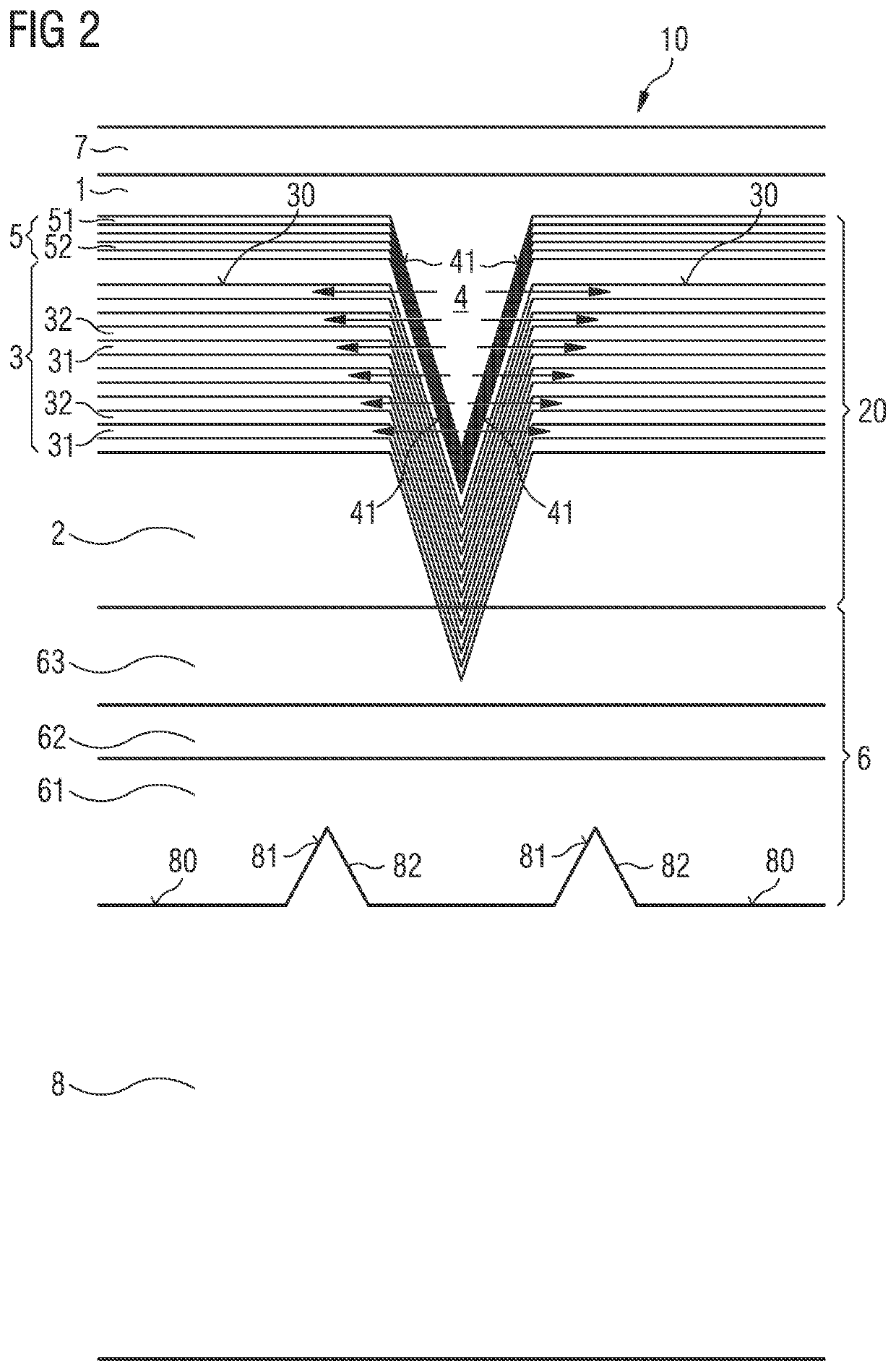
[0014]By means of the recesses, the holes from the p-conducting semiconductor layer can be effectively injected particularly via the obliquely formed facets of the recesses into various regions of the active zone, in particular into various quantum well layers which are arranged one above the other in the vertical direction, as a result of which those quantum well layers arranged comparatively farther from the p-conducting semiconductor layer are better energized, since the holes do not need to be first injected throughout the quantum well layers or the quantum barrier layers arranged closer to the p-conducting semiconductor layer.
[0015]However, if a significant proportion of the holes continues to be injected into the active zone outside the recesses via the main surface of the active zone, i.e., via the c-surface, a particularly uniform distribution of the holes over all quantum well layers of the active zone is difficult to achieve, since the penetration probability of the holes injected via the main surface into the active zone decreases strongly with increasing penetration depth, i.e., with increasing number of quantum barrier layers in the active zone. If the injection of the holes into the active zone via the main surface is hindered or blocked in a targeted manner, the holes that have reached the active zone can essentially only be injected into different quantum well layers of the active zone via the facets of the recesses. The current flow into the active zone is therefore reduced in a targeted manner in the regions on the c-surface. The current flow is increasingly concentrated rather in the regions of recesses. Thus, it can be achieved that the density of the holes remains essentially the same in all quantum well layers, i.e., in the entire active zone. Due to the targeted prevention or blocking of the penetration of the holes into the active zone via the main surface of the active zone, the probability of injection of the positively charged charge carriers into the n-side quantum well layers, which are arranged farther from the p-conducting semiconductor layer, is increased, so that the charge carrier density with regard to the holes is increased in the region of the active zone spaced apart from the p-side, as a result of which the distribution of the holes in the active zone is particularly homogeneous along the vertical direction and the efficiency of the component is thereby increased. Due to such a configuration of the component, the charge carriers are thus homogenized at least along the lateral direction.
[0027]By adjusting the growth conditions in a targeted manner, a considerably thinner layer thickness can be achieved on the facets rather than on the main surface, namely on the c-surface. If the barrier structure is doped, e.g., p-doped, fewer foreign atoms are embedded in the barrier structure in the regions within the recesses due to the polarity of the facets and lower growth rate on the facets. By an epitaxial method, in which the recesses are generated in the transition layer in a targeted manner, the layers of the semiconductor layer sequence or of the barrier structure can be formed in such a way that the layer thickness of these layers on the facets, i.e., in the regions of the recesses, is significantly thinner than on the respective main surface outside the recesses, i.e., on the c-surface. This results in the technical effect that holes can be injected more efficiently into the active zone via the facets of the recesses than via the main surface of the active zone. If the barrier structure containing for instance a plurality of layers arranged alternately one above the other, for example, GaN and AlGaN-based layers, is additionally doped with Si, the barrier structure acts as a hole barrier outside the recesses on the c-surface. Due to the thinner layer thickness and / or lower dopant concentration of the barrier structure within the recesses, the barrier structure can still be formed in such a way that holes can penetrate the barrier structure in the regions of the recesses and easily reach the active zone via the facets.

Problems solved by technology

In optoelectronic components, which are based on a semiconductor material and comprise an active zone, in particular a multiple quantum well structure, it has been shown that charge carriers within the active zone are not evenly distributed over the entire active zone, resulting in efficiency losses of such optoelectronic components.

Method used


Image

  • Component having enhanced efficiency and method for production thereof
  • Component having enhanced efficiency and method for production thereof

Examples


Embodiment Construction

>FIG. 1 shows a component 10 having a carrier 8 on which a semiconductor layer sequence 20 is arranged. The carrier 8 can be a growth substrate on which the semiconductor layer sequence 20 has been epitaxially grown, for example. The semiconductor layer sequence 20 has an active zone 3 which is arranged between a first, for instance p-conducting semiconductor layer 1, and a second, for instance n-conducting semiconductor layer 2. In particular, the active zone 3 is configured for generating electromagnetic radiation during operation of the component 10.

[0037]The active zone 3 has a multiple quantum well structure comprising a plurality of alternating quantum well layers 31 and quantum barrier layers 32. The number of quantum well layers 31 is at least 3 or at least 5 and is, for example, between 3 and 20 inclusive, for instance between 3 and 15 inclusive, for instance 9. The quantum well layers 31 and quantum barrier layers 32 may be based on a III-V compound semiconductor material,...


PUM

PropertyMeasurementUnit
thicknessaaaaaaaaaa
thicknessaaaaaaaaaa
vertical heightaaaaaaaaaa

Abstract

A component having an enhanced efficiency and a method for producing a component are disclosed. In an embodiment, a component includes a semiconductor layer sequence comprising a p-conducting semiconductor layer, an n-conducting semiconductor layer and an active zone located therebetween, wherein the active zone comprises recesses on a side of the p-conducting semiconductor layer, each recess having facets extending obliquely to a main surface of the active zone, and wherein the p-conducting semiconductor layer extends into the recesses, and a barrier structure, wherein the active zone is arranged between the barrier structure and the n-conducting semiconductor layer so that an injection of positively charged charge carriers into the active zone via the main surface is hindered in a targeted manner so that an injection of positively charged charge carriers into the active zone via the facets is promoted.

Description

[0001]This patent application is a national phase filing under section 371 of PCT / EP2017 / 062000, filed May 18, 2017, which claims the priority of German patent application 10 2016 208 717.7, filed May 20, 2016, each of which is incorporated herein by reference in its entirety.TECHNICAL FIELD[0002]The present application relates to a component having uniform current injection and a method for producing a component.BACKGROUND[0003]In optoelectronic components, which are based on a semiconductor material and comprise an active zone, in particular a multiple quantum well structure, it has been shown that charge carriers within the active zone are not evenly distributed over the entire active zone, resulting in efficiency losses of such optoelectronic components.SUMMARY OF THE INVENTION[0004]Embodiments provide a component having increased efficiency. Embodiments further provide an efficient method for producing a component.[0005]According to at least one embodiment of a component, it ha...

Claims


Application Information

Patent Timeline
Patent Type & Authority Patents(United States)
IPC IPC(8): H01L33/24H01L33/06H01L33/00H01L33/18H01L33/32H01L33/38
CPCH01L33/24H01L33/38H01L33/325H01L33/007H01L33/18H01L33/06H01L33/025H01L33/04H01L33/14H01L33/145H01L33/32
Inventor LEHNHARDT, THOMASBERGBAUER, WERNEROFF, JÜRGENLAHOURCADE, LISEDRECHSEL, PHILIPP
Owner OSRAM OLED
Why Eureka
Try Eureka