Imaging apparatus and imaging apparatus control method to reduce power consumption without reduction of number of pixel signals

Active Publication Date: 2020-12-08
SONY SEMICON SOLUTIONS CORP
View PDF11 Cites 0 Cited by
  • Summary
  • Abstract
  • Description
  • Claims
  • Application Information

AI Technical Summary

Benefits of technology

The patent text describes a technology that can help reduce power consumption in a solid-state imaging element without affecting the number of pixel signals. The technology can achieve this by performing advanced digital processing on the pixel signals. The text also mentions that the technology can have various other benefits, which can be any of the benefits described in the patent.

Problems solved by technology

In this configuration, power consumption of the column ADC is particularly greater than in other circuits.

Method used


Image

  • Imaging apparatus and imaging apparatus control method to reduce power consumption without reduction of number of pixel signals
  • Imaging apparatus and imaging apparatus control method to reduce power consumption without reduction of number of pixel signals
  • Imaging apparatus and imaging apparatus control method to reduce power consumption without reduction of number of pixel signals

Examples


first embodiment

1. First Embodiment

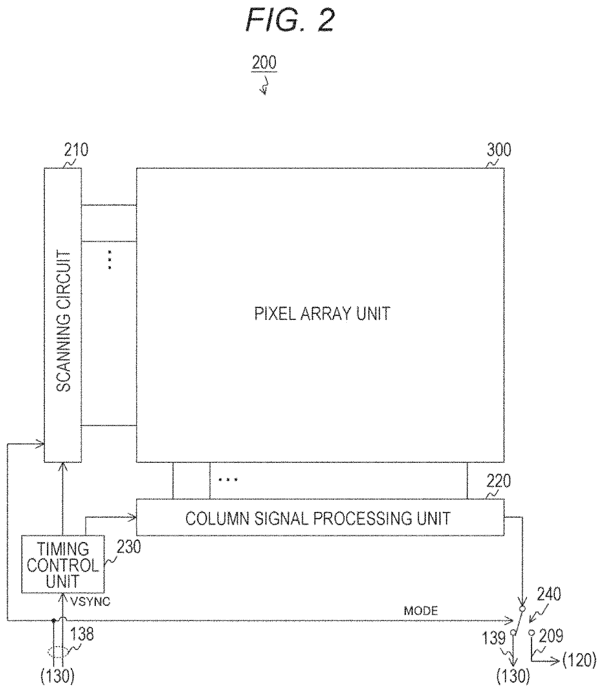
[0040][Configuration Example of Imaging Apparatus]

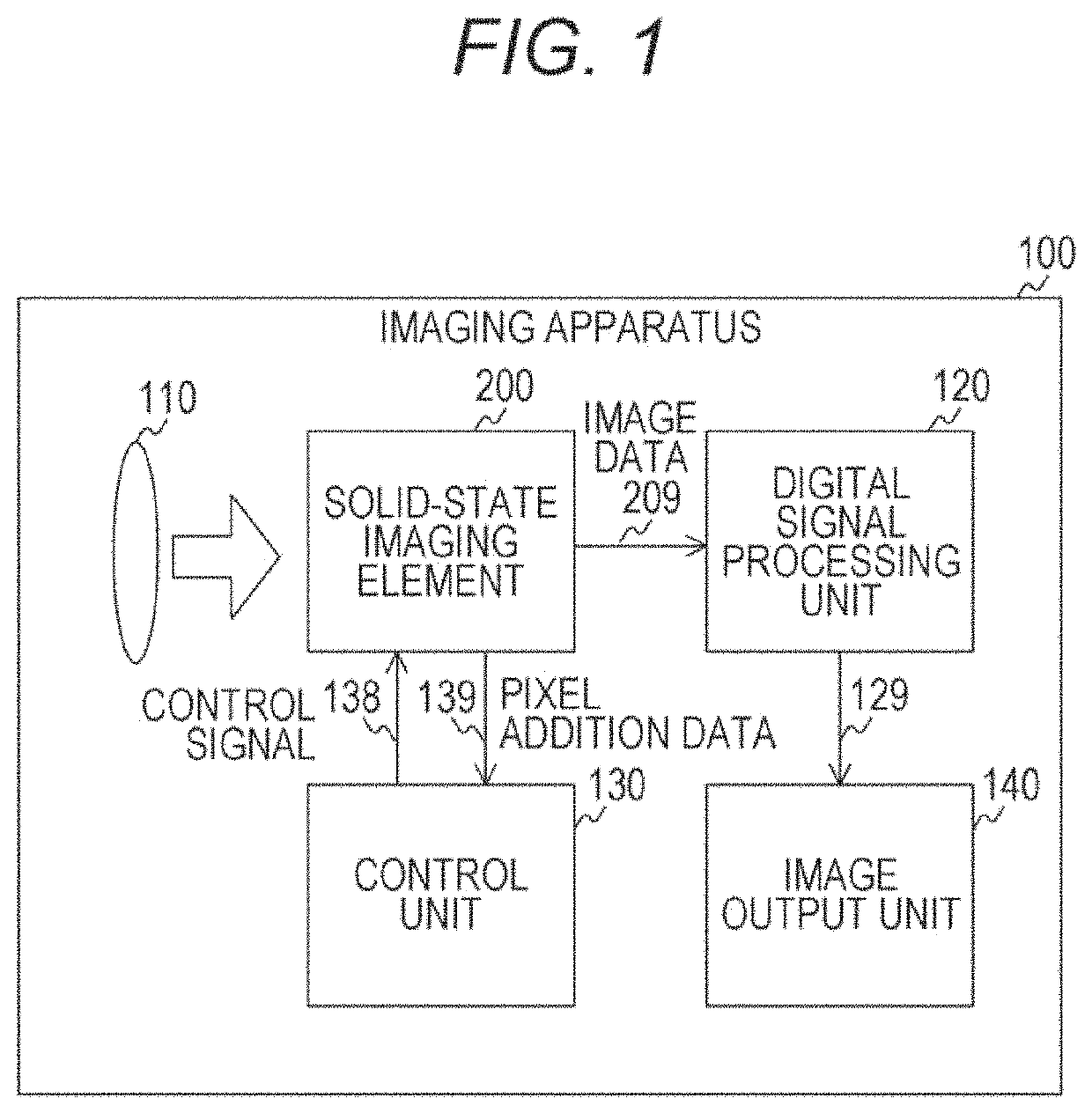
[0041]FIG. 1 is a block diagram illustrating a configuration example of an imaging apparatus 100 according to an embodiment of the present technology. The imaging apparatus 100 is an apparatus having an imaging function, and includes an imaging lens 110, a solid-state imaging element 200, a digital signal processing unit 120, a control unit 130, and an image output unit 140. Assumable examples of the imaging apparatus 100 include a digital camera, a smartphone, a personal computer, and the like. Examples of digital camera include a monitoring camera, an Intelligent Transport Systems (ITS) camera, a home camera, an action camera, an Internet of Things (IoT) camera, and the like.

[0042]The imaging lens collects light from a subject and guides the light to the solid-state imaging element 200.

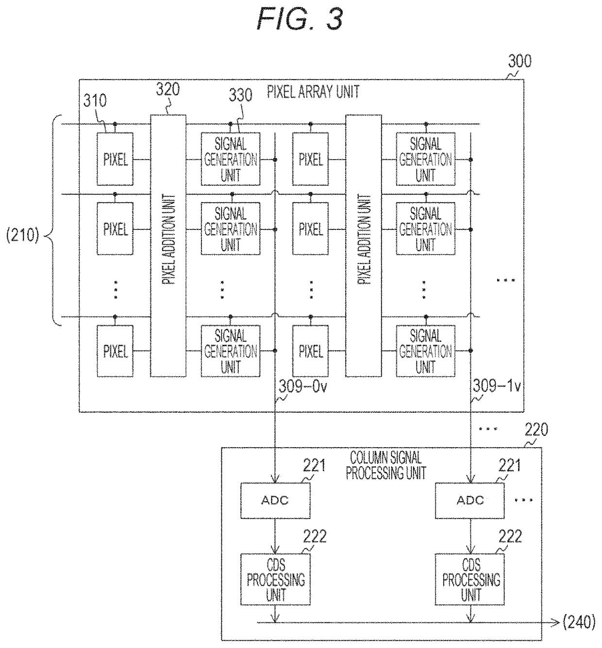
[0043]The solid-state imaging element 200 captures image data in accordance with a control signal from the control unit 130. Here...

second embodiment

2. Second Embodiment

[0108]In the first embodiment described above, the imaging apparatus 100 determines the presence or absence of motion of the subject and switches the operation mode to the non-addition mode when motion is present. However, in a case where the imaging apparatus 100 is used for imaging an object (such as an automobile) moving at a constant speed or more in the non-addition mode, the mode might be switched to the non-addition mode even when a subject (such as plants) other than the object moves, leading to a possible concern that the power consumption cannot be sufficiently reduced. Therefore, in a second embodiment, the object speed is further measured in the pixel addition mode. That is, the imaging apparatus 100 according to the second embodiment is different from the first embodiment in that the speed of the object is measured in the pixel addition mode.

[0109]FIG. 12 is a graph illustrating an example of trajectories of past addition data and current addition da...

third embodiment

3. Third Embodiment

[0128]In the second embodiment described above, the imaging apparatus 100 measures the movement speed in the row direction. However, depending on the installation position of the imaging apparatus 100, the subject might move in the depth direction, leading to a possible concern that accurate measurement of the movement speed cannot be made in some cases. Therefore, the imaging apparatus 100 according to a third embodiment measures the movement speed in the depth direction. That is, the imaging apparatus 100 according to the third embodiment is different from the second embodiment in that the movement speed in the depth direction is measured.

[0129]FIG. 17 is a view illustrating an example of a past frame 550 according to the third embodiment of the present technology. The third embodiment assumes that the imaging apparatus 100 is installed at an upper side of the road and that the road extends in an optical axis direction (in other words, the depth direction). The ...


PUM


Abstract

Reducing power consumption without reducing the number of pixel signals in a solid-state imaging element that performs AD conversion of a pixel signal. A pixel array unit includes a plurality of lines each having a plurality of pixels arranged in a predetermined direction. A scanning circuit sequentially selects the plurality of lines and then controls to output an analog signal from each of the pixels within the selected line in a non-addition mode, and simultaneously selects the plurality of lines and controls to add up the analog signals of each of the pixels arranged in a direction perpendicular to the predetermined direction and output the added signals in a pixel addition mode. The analog-to-digital conversion unit converts each of the analog signals into a digital signal. The control unit performs control of switching from one of the pixel addition mode and the non-addition mode to the other on the basis of the digital signal.

Description

CROSS REFERENCE TO RELATED APPLICATIONS[0001]This application is a U.S. National Phase of International Patent Application No. PCT / JP2017 / 036631 filed on Oct. 10, 2017, which claims priority benefit of Japanese Patent Application No. JP 2017-006086 filed in the Japan Patent Office on Jan. 17, 2017. Each of the above-referenced applications is hereby incorporated herein by reference in its entirety.TECHNICAL FIELD[0002]The present technology relates to an imaging apparatus and an imaging apparatus control method. More specifically, the present invention relates to an imaging apparatus that converts an analog pixel signal into a digital signal, and a method for controlling the imaging apparatus.BACKGROUND ART[0003]Conventionally, an apparatus including an imaging function has been using a solid-state imaging element for capturing image data. For example, the solid-state imaging element includes: a pixel array including pixels arranged in a two-dimensional lattice pattern; a scanning c...

Claims


Application Information

Patent Timeline
IPC IPC(8): H04N5/335H04N5/3745H04N5/369H04N5/378H04N5/343
CPCH04N5/343H04N5/378H04N5/37455H04N5/3698H04N25/42H04N25/46H04N25/709H04N25/772H04N25/75
Inventor HOSHINO, KAZUHIROIINUMA, TAKAHIRO
Owner SONY SEMICON SOLUTIONS CORP
Why Eureka
Try Eureka