
Optical sensor and method for forming same

a technology of optical sensors and optical sensors, applied in the field of optical sensors, can solve the problems of reducing the light absorption efficiency, the thickness of the actual optical device cannot be increased without limitation, and the manufacturing cost of silicon crystals with a large l and a high purity, and achieves the effect of simple texture structure and high photoelectric conversion efficiency

Active Publication Date: 2020-12-29
NEC CORP
View PDF22 Cites 0 Cited by
  • Summary
  • Abstract
  • Description
  • Claims
  • Application Information

AI Technical Summary

Benefits of technology

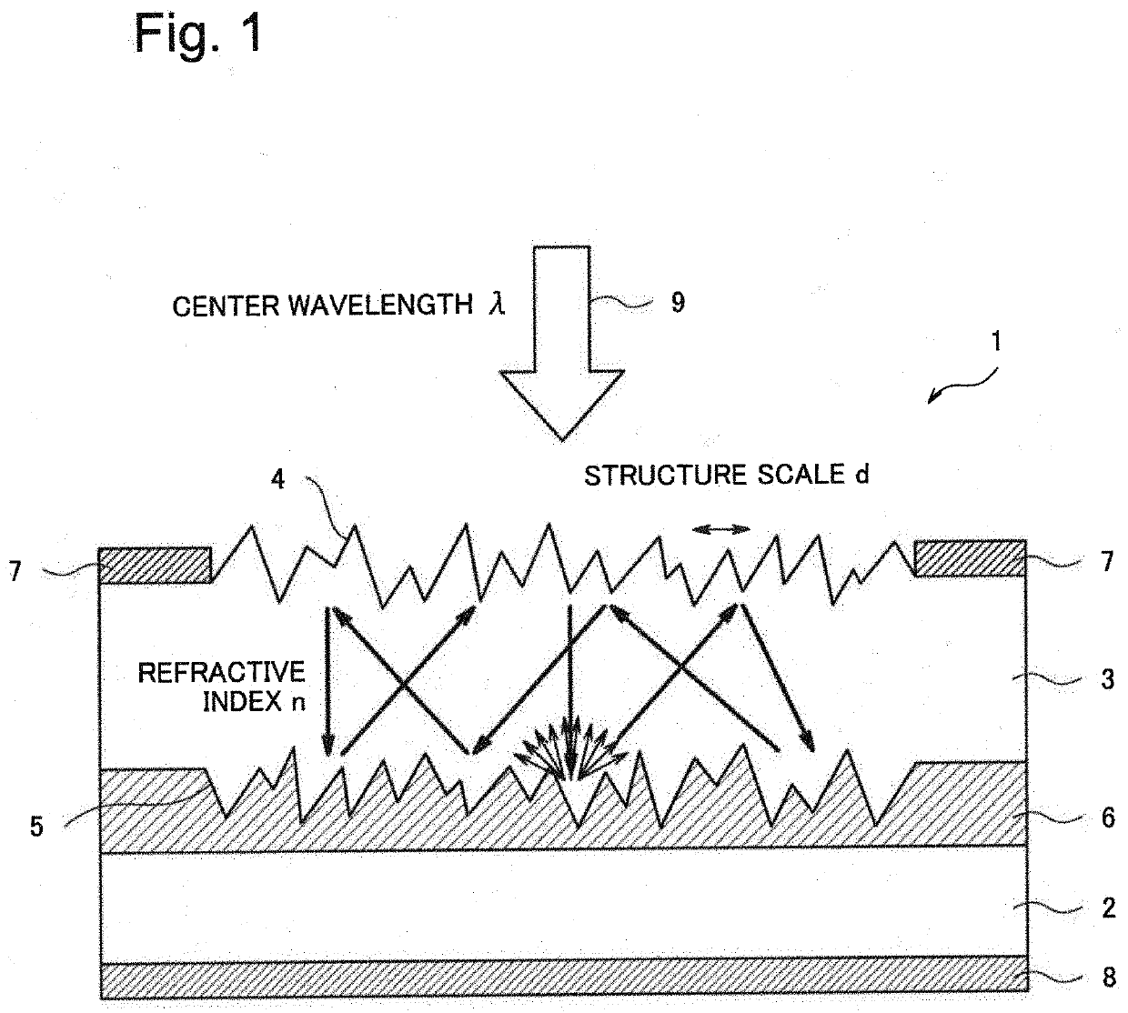
The invention provides an optical sensor that can capture a lot of light using a simple structure. This makes it easy to form the sensor and increase its efficiency.

Problems solved by technology

However, an actual optical device cannot increase the thickness L without limitation.
For example, a solar cell has an issue of a high manufacturing cost of a silicon crystal with a large L and a high purity, and therefore it is required to increase a light absorption probability with as thin a silicon crystal as possible.
There is, however, an issue that thinning of an absorption medium directly translates to a decrease in a light absorption efficiency.
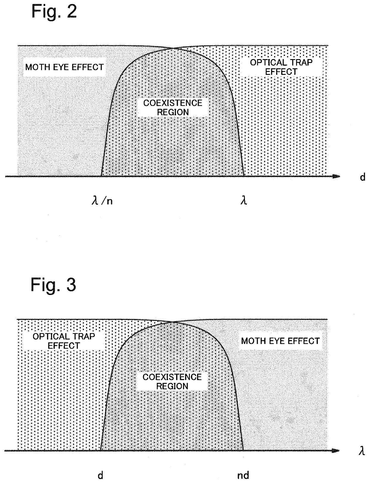
However, as described later, a structure scale of a texture surface offering these effects is substantially different, and thus there is an issue that it is difficult to enhance absorption of incident light into a solar cell in a wide wavelength region by using a single texture structure.

Method used


Image

  • Optical sensor and method for forming same
  • Optical sensor and method for forming same
  • Optical sensor and method for forming same

Examples


first example embodiment

[0041][Description of Structure]

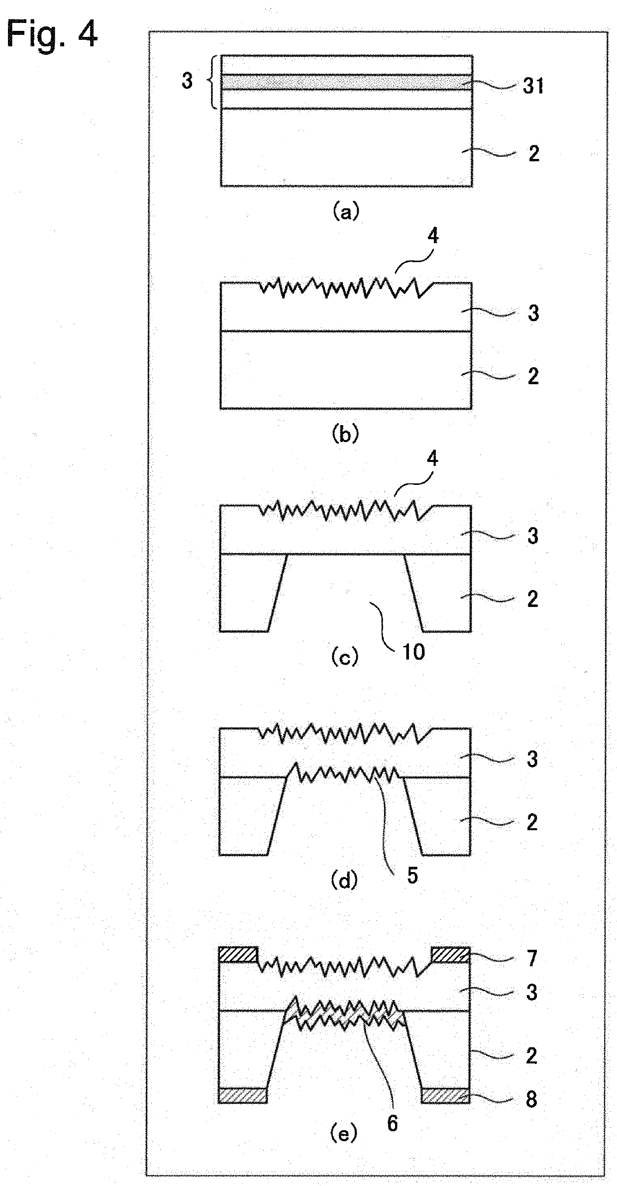
[0042]FIG. 1 is a sectional view schematically illustrating an optical sensor according to a first example embodiment of the present invention. An optical sensor 1 according to this example embodiment is laminated on a substrate 2 as illustrated in FIG. 1 and includes a light absorption medium 3 having a refractive index n and absorbing light of a target center wavelength λ. A thickness of the light absorption medium 3 is sufficiently less than a light transmission length (an inverse of an absorption coefficient). The substrate 2 and the light absorption medium 3 are properly doped. It is possible to pull out a photocarrier generated via light absorption by giving a proper bias to a lower electrode 8 arranged in a lower part of the substrate 2 and an upper electrode 7 arranged in an upper part of the light absorption medium 3. When the substrate 2 is made of GaAs, an n-type semiconductor substrate is formed for example by doping Si about 1 to 3×10⁻¹⁸ ...

second example embodiment

[0075]FIG. 6 is a sectional view illustrating an optical sensor according to a second example embodiment of the present invention.

[0076]An optical sensor 100 according to the example embodiment includes a light absorption medium 300 having a refractive index n and a thickness sufficiently less than a light transmission length. The light absorption medium 300 has a light incident surface texture structure 40. Assuming that an observation target center wavelength is λ, the texture structure has a random surface direction and a typical structure scale d defined as in (λ / n)60 is arranged between the light absorption medium 300 and a substrate 20 in the example embodiment. The light reflector 60 desirably has a high reflectivity.

[0077]In the example embodiment, as in the first example embodiment, light incident having a target center wavelength λ from the vertical directional vicinity (incident light 90) is less reflected at an incident surface by a moth eye effect. At a light incident s...


PUM

PropertyMeasurementUnit
lengthaaaaaaaaaa
refractive indexaaaaaaaaaa
wavelengthaaaaaaaaaa

Abstract

In order to provide an optical sensor that is capable of obtaining both an optical trap effect and a moth eye effect with a single texture structure, a semiconductor optical sensor according to the present invention includes a light absorption medium that has a refractive index n and a thickness sufficiently less than a light transmission length, wherein the center wavelength to be observed is defined as λ. The semiconductor optical sensor is characterized by: having, in a light incident surface, a texture structure having a random surface direction and a typical structure scale d defined as in (λ / n).

Description

CROSS REFERENCE TO RELATED APPLICATIONS[0001]This application is a National Stage of International Application No. PCT / JP2017 / 033817, filed Sep. 20, 2017, claiming priority to Japanese Patent Application No. 2016-188123, filed Sep. 27, 2016, the contents of all of which are incorporated herein by reference in their entirety.TECHNICAL FIELD[0002]The present invention relates to an optical sensor, in particular to an optical sensor aiming to acquire information on a target by receiving light and a method for forming the same.BACKGROUND ART[0003]Photoelectric conversion elements have been used for a plurality of purposes. Important examples include a solar cell aiming to collect useful energy from sunlight and an optical sensor aiming to acquire useful information related to a target from observation light, such as a sensing device used for IoT (Internet of Things).[0004]An important performance specification of these photoelectric conversion elements is a photoelectric conversion effi...

Claims


Application Information

Patent Timeline
Patent Type & Authority Patents(United States)
IPC IPC(8): H01L31/0236H01L31/0224H01L31/0352H01L31/18H01L31/0232H01L31/10
CPCH01L31/10H01L31/022408H01L31/02327H01L31/02366H01L31/184H01L31/035218H01L31/02363H01L31/03046
Inventor NAMBU, YOSHIHIRO
Owner NEC CORP
Learn More