Method of fabricating MEMS devices using plasma etching and device therefor

a technology of plasma etching and mems, applied in the field of mems (microelectromechanicalsystems), can solve the problems of increasing cost, focusing on mems development, and reducing the focus of mems development, so as to improve the reliability of such mems structural components, improve the long-term reliability of mems components, and improve the effect of the reliability of such structural components

Active Publication Date: 2021-02-09
MOVELLA INC
View PDF90 Cites 0 Cited by
  • Summary
  • Abstract
  • Description
  • Claims
  • Application Information

AI Technical Summary

Benefits of technology

[0008]In an embodiment, the present invention provides a method for fabricating an MEMS sensor device. The method can include the following steps: providing a substrate, forming an IC layer overlying the substrate, forming an oxide layer overlying the IC layer, forming a meta layer coupled to the IC layer through the oxide layer, coupling a MEMS layer having a pair of designated sense electrode portions and a designated proof mass portion overlying the oxide layer, forming a via structure within each of the designated sense electrode portions, and etching the MEMS layer to form a pair of sense electrodes and a proof mass from the designated sense electrode portions and proof mass portions, respectively. The via structure can include a ground post and the proof mass can include a sense comb. The MEMS sensor device formed using this method can result is more well-defined edges of the proof mass structure.
[0009]Embodiments of the present invention provide a means to improve an etching process used to define a MEMS layer to form MEMS structural components. Such embodiments are believed to also improve the long-term reliability of the MEMS components. In conventional MEMS devices, it was not considered necessary to connect the MEMS conductive moving structures before patterning (i.e. MEMS etching process). By connecting the “conductive material” to a ground post through a via structure, the pattering of these structures results in a good and controlled profile.
[0010]Embodiments of the present invention also provide additional means to further improve the reliability of such MEMS structural components. In various embodiments, structures are formed within a capping layer above moving portions of a MEMS layer as well as non-moving portions of the MEMS layer. Such embodiments help reduce deflection of the capping layer, under external pressure, and provide greater performance reliability.

Problems solved by technology

Although highly successful, ICs and in particular MEMS still have limitations.
Similar to IC development, MEMS development, which focuses on increasing performance, reducing size, and decreasing cost, continues to be challenging.
Additionally, applications of MEMS often require increasingly complex microsystems that desire greater computational power.
Unfortunately, such applications generally do not exist.

Method used


Image

  • Method of fabricating MEMS devices using plasma etching and device therefor
  • Method of fabricating MEMS devices using plasma etching and device therefor
  • Method of fabricating MEMS devices using plasma etching and device therefor

Examples


Embodiment Construction

[0019]The present invention is directed to MEMS (Micro-Electro-Mechanical-Systems). More specifically, embodiments of the invention provide methods for fabricating an integrated MEMS device, including MEMS sensors and the like, and a resulting device structure. Merely by way of example, the MEMS device can include at least an accelerometer, a gyroscope, a magnetic sensor, a pressure sensor, a microphone, a humidity sensor, a temperature sensor, a chemical sensor, a biosensor, an inertial sensor, and others. But it will be recognized that the invention has a much greater range of applicability.

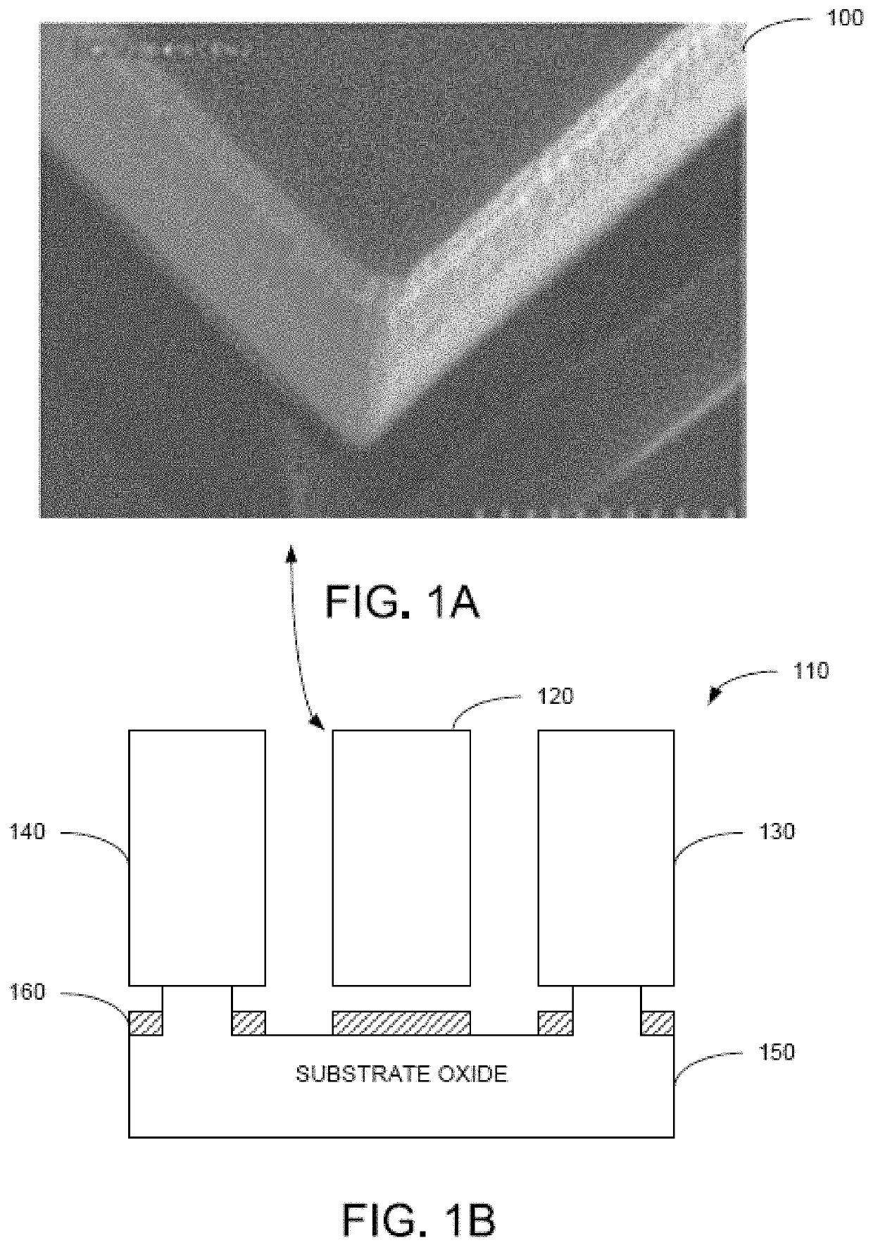
[0020]FIG. 1A shows an SEM (Scanning Electron Microscope) image 100 of a proof mass edge according to an embodiment of the present invention. This image shows an edge portion of a proof mass structure for a MEMS inertial sensor. As shown, the edge shows a serious etching defects when a MEMS via process is not included. According to an embodiment, these kinds of defects can arise from performing...


PUM

PropertyMeasurementUnit
massaaaaaaaaaa
heightaaaaaaaaaa
metallicaaaaaaaaaa

Abstract

A method for fabricating a MEMS sensor device. The method can include providing a substrate, forming an IC layer overlying the substrate, forming an oxide layer overlying the IC layer, forming a metal layer coupled to the IC layer through the oxide layer, forming a MEMS layer having a pair of designated sense electrode portions and a designated proof mass portion overlying the oxide layer, forming a via structure within each of the designated sense electrode portions, and etching the MEMS layer to form a pair of sense electrodes and a proof mass from the designated sense electrode portions and proof mass portions, respectively. The via structure can include a ground post and the proof mass can include a sense comb. The MEMS sensor device formed using this method can result is more well-defined edges of the proof mass structure.

Description

CROSS-REFERENCES TO RELATED APPLICATIONS[0001]The present application claims priority to and incorporates by reference, for all purposes, commonly-owned U.S. Provisional App. 61 / 953,699, filed on Mar. 14, 2014. The present application also incorporates by reference, for all purposes, the following commonly-owned pending patent applications: U.S. patent application Ser. No. 14 / 507,177, filed Oct. 4, 2014, and U.S. patent application Ser. No. 13 / 788,503, filed Mar. 7, 2013.BACKGROUND OF THE INVENTION[0002]The present invention is directed to MEMS (Micro-Electro-Mechanical-Systems). More specifically, embodiments of the invention provide methods and structures for improving integrated MEMS devices, including MEMS sensors and the like.[0003]Research and development in integrated microelectronics have continued to produce astounding progress in CMOS and MEMS. CMOS technology has become the predominant fabrication technology for integrated circuits (IC). MEMS, however, continues to rely u...

Claims


Application Information

Patent Timeline
Patent Type & Authority Patents(United States)
IPC IPC(8): B81B7/00B81C1/00
CPCB81B7/0006B81C1/00531B81B2201/0235B81B2201/0242B81B2203/0307B81B2203/04B81C2203/0109B81B3/0051B81B7/0077G01P15/0802G01P15/125G01P2015/0871
Inventor CHUANG, BEN (WEN-PIN)KUO, M H (MING-HONG)CHEN, W J (WEN-CHIH)LEE, TSE-HSI “TERRENCE”
Owner MOVELLA INC
Why Eureka
Try Eureka