Array substrate and display device comprising same
a display device and substrate technology, applied in semiconductor devices, instruments, electrical devices, etc., can solve the problems of reducing the effect of defects on product yield, affecting the product yield, and easily forming defects, so as to reduce the stress on at least one metal trace, less tensile stress, and more resistant to bending
- Summary
- Abstract
- Description
- Claims
- Application Information
AI Technical Summary
Benefits of technology
Problems solved by technology
Method used
Image


Examples
Embodiment Construction
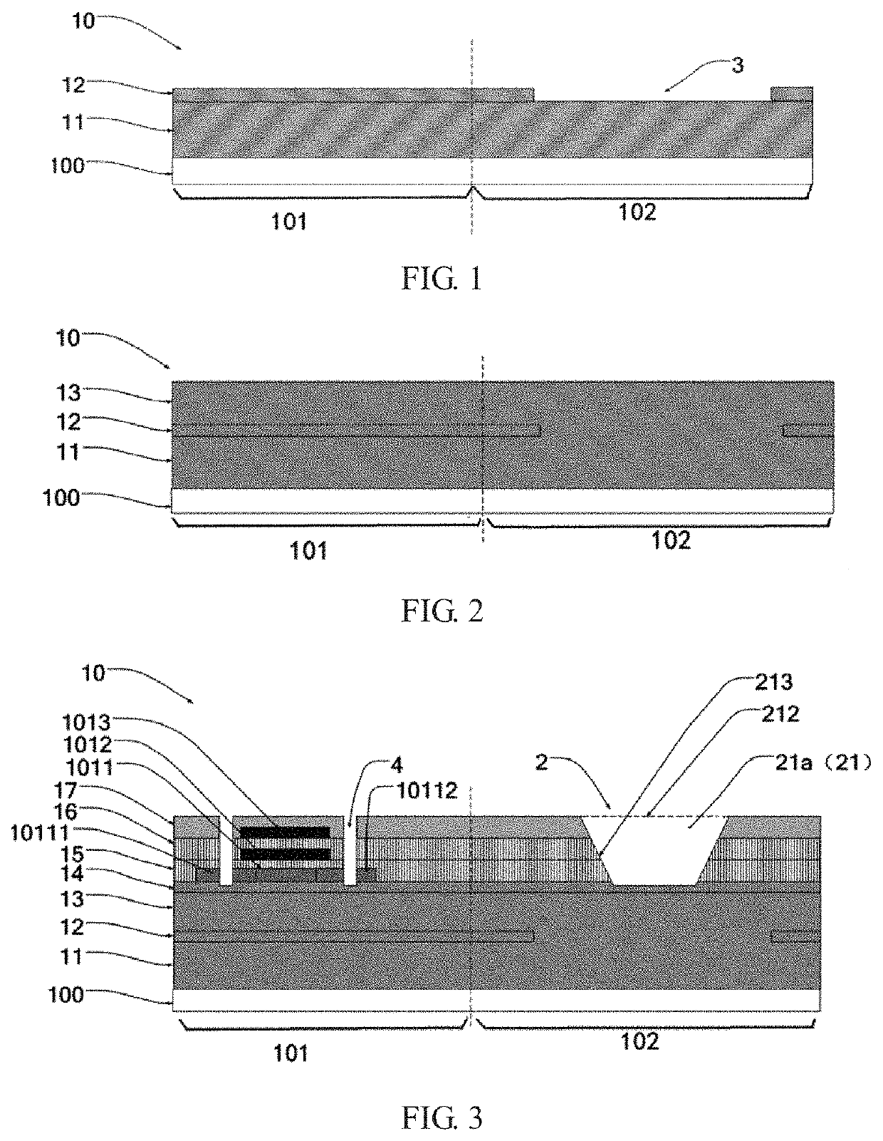
[0029]The embodiments of the present invention are described in detail below, and the examples of the embodiments are illustrated in the drawings, wherein the same or similar reference numerals indicate the same or similar elements or elements having the same or similar functions. The embodiments described below with reference to the drawings are intended to be illustrative of the invention and are not to be construed as limiting.
[0030]Description of following embodiment, with reference to accompanying drawings, is used to exemplify specific embodiments which may be carried out in the present disclosure. Directional terms mentioned in the present disclosure, such as “top”, “bottom”, “front”, “back”, “left”, “right”, “inside”, “outside”, “side”, etc., are only used with reference to orientation of the accompanying drawings. Therefore, the directional terms are intended to illustrate, but not to limit, the present disclosure. In the drawings, components having similar structures are d...
PUM
| Property | Measurement | Unit |
|---|---|---|
| thickness | aaaaa | aaaaa |
| thickness | aaaaa | aaaaa |
| width | aaaaa | aaaaa |
Abstract
Description
Claims
Application Information