Method for bonding by direct adhesion

a direct adhesion and bonding technology, applied in the direction of basic electric elements, semiconductor/solid-state device manufacturing, electrical equipment, etc., can solve the problems of changing the adhesion of the bonding interface, the prior art process is not completely satisfactory, and the waiting time is stringen

Active Publication Date: 2021-03-23
COMMISSARIAT A LENERGIE ATOMIQUE ET AUX ENERGIES ALTERNATIVES
View PDF3 Cites 0 Cited by
  • Summary
  • Abstract
  • Description
  • Claims
  • Application Information

AI Technical Summary

Benefits of technology

[0026]Thus, one advantage afforded by a dedicated layer is that it makes it possible to provide the hydrophobic character regardless of the material of the first and second substrates.
[0029]Thus, one advantage afforded by a hydrophobic treatment to the lateral edges is simplicity of implementation. It is not necessary to form, and then remove, a dedicated layer.
[0033]Thus, one advantage afforded by such a heat treatment is that it slows the kinetics of the ingress of water into the bonding interface, and does so without closing off the bonding interface, i.e. water molecules are still able to enter the bonding interface where empty spaces remain. Such a heat treatment allows the waiting time before carrying out step c) to be longer without risking damage to the bonding interface.
[0037]Thus, one advantage afforded by such waiting times is that step c) is carried out early enough, i.e. before the kinetics of the ingress of water into the bonding interface take effect.

Problems solved by technology

This ingress of water molecules into the bonding interface leads to the formation of defects and to the adhesion of the bonding interface changing.
Such a prior art process is therefore not completely satisfactory inasmuch as it appears to be necessary:(i) either to control the atmosphere (in particular the humidity level) under which step b0) is carried out until step c0) is to be carried out;(ii) or to carry out step c0) soon after step b0), i.e. faster than the kinetics of the ingress of water into the bonding interface, which means stringent management of the waiting time for the bonded substrates.
Furthermore, according to the envisaged application, steps that come between steps b0) and c0) are likely to have to be carried out in an environment that is very wet, and hence potentially damaging for the bonding interface.

Method used


Image

  • Method for bonding by direct adhesion
  • Method for bonding by direct adhesion

Examples


implementation example no.1

Implementation Example No. 1

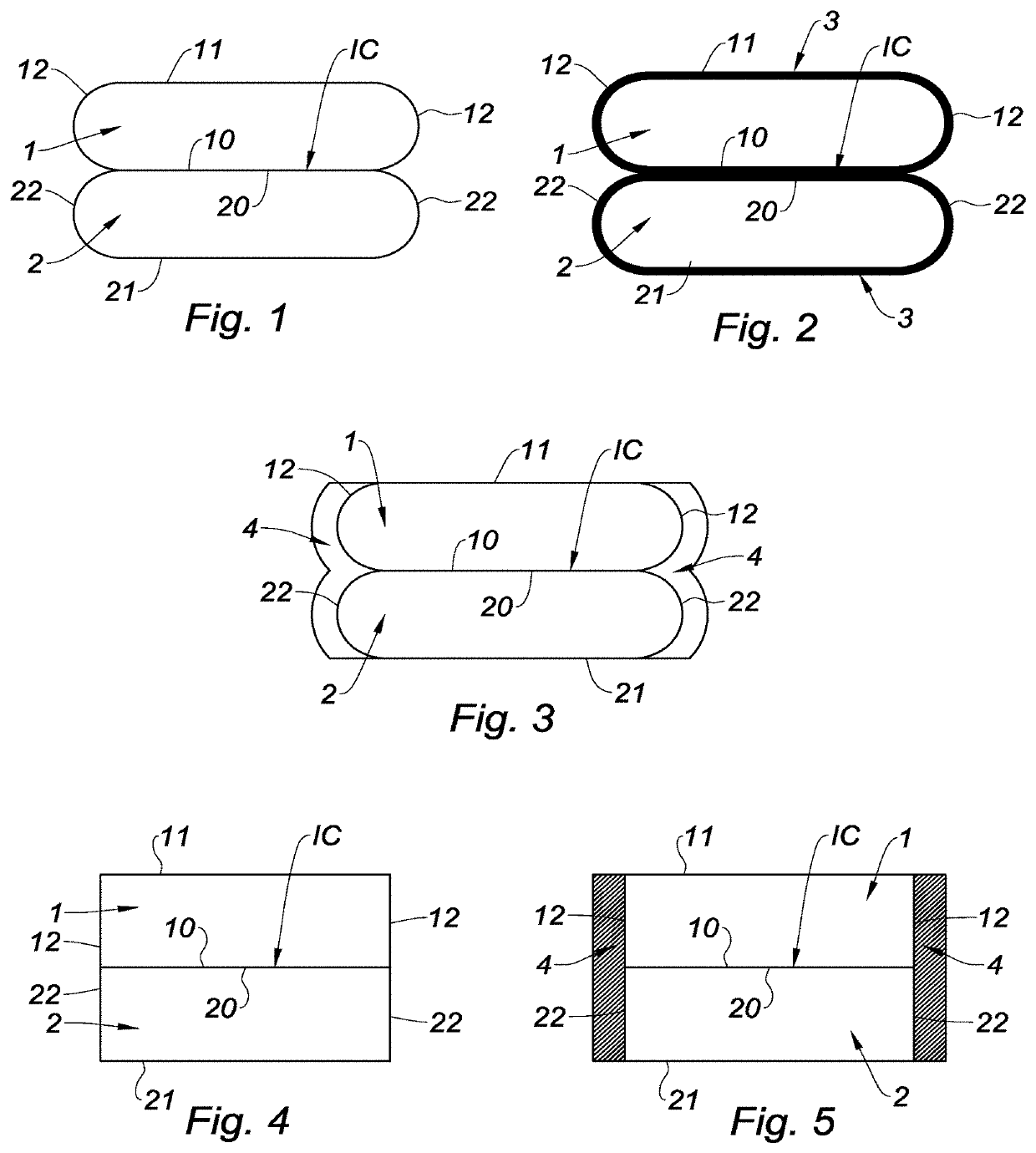
[0075]The first and second substrates 1, 2 are two (001) silicon wafers of 200 mm in diameter and 725 μm in thickness. The first and second substrates 1, 2 are cleaned and hydrolysed in baths of ozonated deionized water and in an APM (ammonia-peroxide mixture) solution at 70° C. so that the bonding surfaces are hydrophilic. The first and second substrates 1, 2 are direct-bonded at ambient temperature and at ambient pressure.

[0076]Step c) is carried out by forming a fluorinated coating on the lateral edges 12, 22 of the first and second substrates 1, 2 on either side of the bonding interface IC, as well as on the second surfaces 11, 21 of the first and second substrates 1, 2. In order to achieve this, step c) is carried out by turning the bonded first and second substrates 1, 2 in a bath of Novec™ 2702. Excess fluorinated coating may be removed using a solvent (e.g. Novec™ 7200) and by rinsing with isopropyl alcohol (IPA). This fluorinated coating may be r...

implementation example no.2

Implementation Example No. 2

[0094]The first and second substrates 1, 2 are two (001) silicon wafers of 200 mm in diameter and 725 μm in thickness. The first and second substrates 1, 2 are cleaned and hydrolysed in baths of ozonated deionized water and in an APM (ammonia-peroxide mixture) solution at 70° C. so that the bonding surfaces are hydrophilic. The first and second substrates 1, 2 are direct-bonded at ambient temperature and at ambient pressure.

[0095]Step c) is carried out by forming a fluorinated coating on the lateral edges 12, 22 of the first and second substrates 1, 2 on either side of the bonding interface IC, as well as on the second surfaces 11, 21 of the first and second substrates 1, 2. In order to achieve this, step c) is carried out while turning the bonded first and second substrates 1, 2 in a bath of Novec™ 1700. Excess fluorinated coating may be removed using a solvent (e.g. Novec™ 7200 or 7100) and by rinsing with isopropyl alcohol (IPA). This fluorinated coati...

implementation example no.3

Implementation Example No. 3

[0096]The first and second substrates 1, 2 are two (001) silicon wafers of 200 mm in diameter and 725 μm in thickness. The first and second substrates 1, 2 are cleaned and hydrolysed in baths of ozonated deionized water and in an APM (ammonia-peroxide mixture) solution at 70° C. so that the bonding surfaces are hydrophilic. The first and second substrates 1, 2 are direct-bonded at ambient temperature and at ambient pressure.

[0097]Step c) is carried out by adding paraffin wax to the lateral edges 12, 22 of the first and second substrates 1, 2 on either side of the bonding interface IC, as well as to the second surfaces 11, 21 of the first and second substrates 1, 2. In order to achieve this, step c) is carried out by turning the bonded first and second substrates 1, 2 in a bath of molten paraffin wax. The paraffin wax may be removed later by means of a solvent such as acetone.


PUM

PropertyMeasurementUnit
temperatureaaaaaaaaaa

Abstract

A process includes the successive steps of: a) providing first and second substrates, each including a first surface and an opposite, second surface, lateral edges connecting the first and second surfaces, b) bonding the first substrate to the second substrate by direct bonding with the first surfaces of the first and second substrates so as to form a bonding interface (IC), and making the lateral edges of the first and second substrates hydrophobic on either side of the bonding interface (IC).

Description

TECHNICAL FIELD[0001]The invention relates to the technical field of attaching two substrates to one another by direct bonding.[0002]A particular application of the invention is in the transfer of thin layers for fabricating electronic devices.STATE OF THE PRIOR ART[0003]A direct bonding process known from the prior art, in particular from the document by M. Tedjini et al., “Interface water diffusion in silicon direct bonding”, Appl. Phys. Lett., 109, 111603, 2016 (D1 hereinafter), includes the steps of:[0004]a0) providing first and second substrates, each comprising a first surface and an opposite, second surface;[0005]b0) bonding the first substrate to the second substrate by direct bonding with the first surfaces of the first and second substrates so as to form a bonding interface.[0006]D1 teaches that the bonding interface is not isolated from the atmosphere under which step b0) is carried out. In particular, water molecules are able to enter the bonding interface, following cer...

Claims


Application Information

Patent Timeline
Patent Type & Authority Patents(United States)
IPC IPC(8): H01L21/18H01L21/20H01L21/67
CPCH01L21/187H01L21/2007H01L21/67092
Inventor FOURNEL, FRANKLARREY, VINCENTMORALES, CHRISTOPHETEDJINI, MARWAN
Owner COMMISSARIAT A LENERGIE ATOMIQUE ET AUX ENERGIES ALTERNATIVES
Why Eureka
Try Eureka