Supercharge Your Innovation With Domain-Expert AI Agents!

High information content imaging using Mie photo sensors

a technology of photo sensors and high information content, applied in the field of photosensitive devices, can solve the problems of signal-to-noise ratio, dynamic range, depth of field, depth of focus, etc., and achieve the effect of reducing the number of sensors, and improving the quality of images

Active Publication Date: 2021-05-04
PIXELEXX SYST INC
View PDF1 Cites 0 Cited by
  • Summary
  • Abstract
  • Description
  • Claims
  • Application Information

AI Technical Summary

Benefits of technology

This patent is about using Mie photo sensors to create pixels that can be connected to control electronics to create an image sensor. These pixels work better than conventional image sensors. The technical effect is that image sensors made with Mie photo sensors are more effective and better than other types of image sensors.

Problems solved by technology

Many attempts at designing photo sensor to minimize their physical size, but the resulting sensors often have many drawbacks.
For example, the signal-to-noise ratio, dynamic range, depth of field, and depth of focus, all deteriorate when generating images with photo sensors of decreased size.

Method used


Image

  • High information content imaging using Mie photo sensors
  • High information content imaging using Mie photo sensors
  • High information content imaging using Mie photo sensors

Examples


Embodiment Construction

I. Introduction

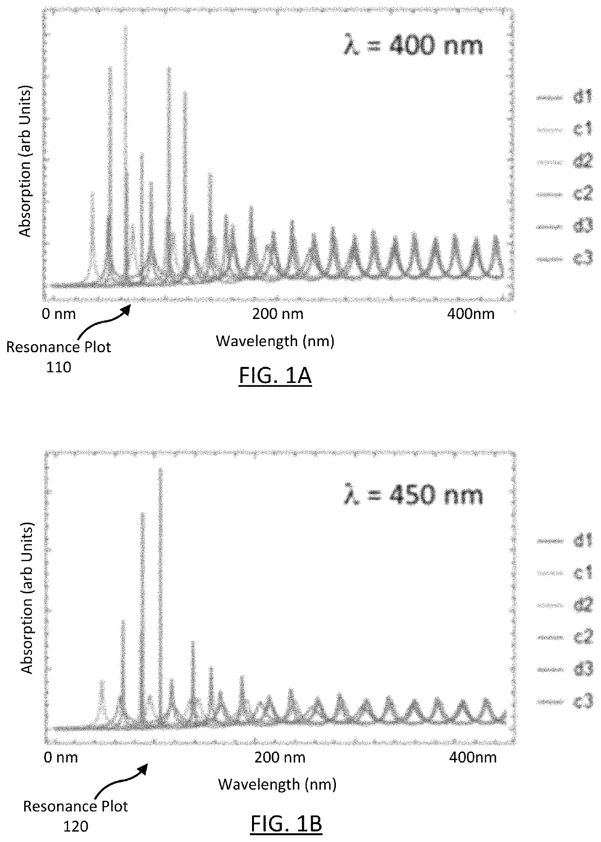
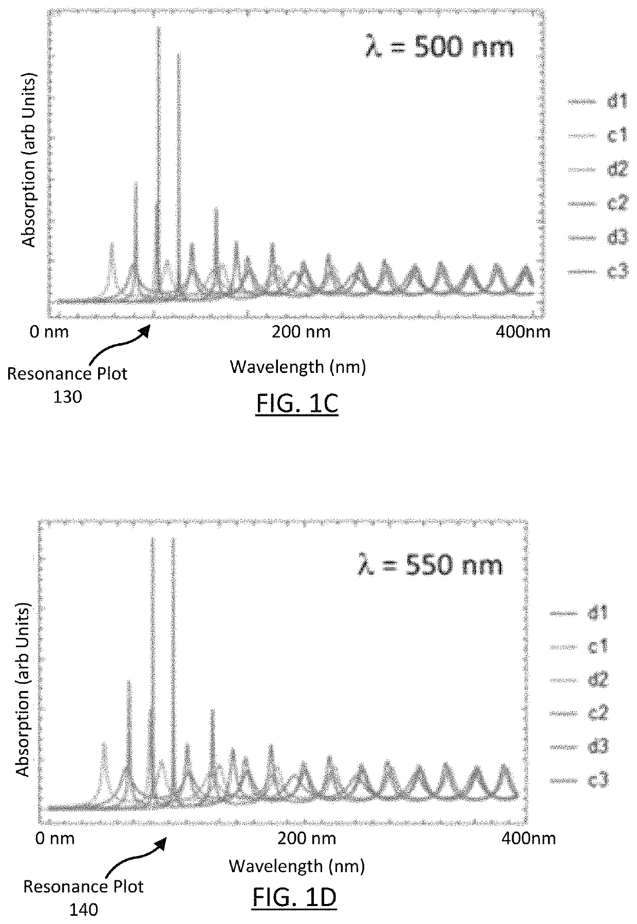
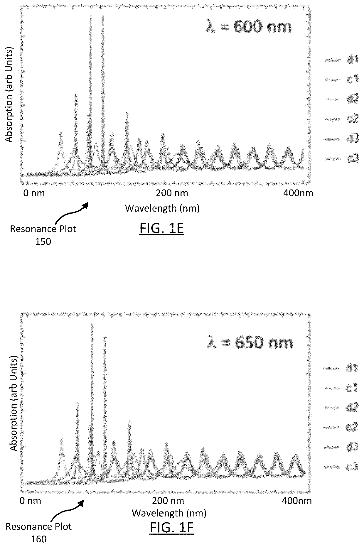
[0030]Photo sensor arrays are composed of a surface including a number of pixels where each pixel may comprise a photo sensor and signal collection electronics that are, generally, approximately co-located with each photo sensor. Each pixel operates by detecting photons at particular wavelengths and then generating an electrical charge, voltage, or resistance that is related to the number of photons detected at each pixel. This charge, voltage, or resistance is then measured, digitized, and used to construct an image of the object, scene, or phenomenon that emitted or reflected the photons. Photo sensors can also be deployed for imaging as single detector or as an array of detectors.

[0031]Future photo sensor technology adoption may be fueled by, for example, three primary ideas: i) image quality (e.g., resolution, low light performance, multispectral imaging, etc.), ii) pixel size in three-dimensions, and, 3) device functionality (e.g., high-speed video, image analysi...


PUM

PropertyMeasurementUnit
heightaaaaaaaaaa
heightaaaaaaaaaa
feature sizeaaaaaaaaaa

Abstract

A Mie photo sensor is described. A Mie photo sensor is configured to leverage Mie scattering to implement a photo sensor having a resonance. The resonance is based on various physical and material properties of the Mie photo sensor. In an example, a Mie photo sensor includes a layer of semiconductor material with one or more mesas. Each mesa of semiconductor material may include a scattering center. The scattering center is formed by the semiconductor material of the mesa being at least partially surround by a material with a different refractive index than the semiconductor material. The abutting refractive index materials create an interface that forms a scattering center and localizes the generation of free carriers during Mie resonance. One or more electrical contacts may be made to the mesa to measure the electrical properties of the mesa.

Description

CROSS REFERENCE TO RELATED APPLICATIONS[0001]This application claims the benefit of U.S. Provisional application No. 62 / 720,002 filed on Aug. 20, 2018, which is incorporated in its entirety by this reference.GOVERNMENT RIGHTS LEGEND[0002]This invention was made with government support under Federal Award Identification Number 1660145 awarded by the National Science Foundation. The government has certain rights in the invention.BACKGROUND1. Technical Field[0003]This disclosure relates generally to a photo-sensitive device, and more particularly, to an array of photo-sensitive devices for generating images.2. Description of the Related Art[0004]Conventional photo sensors operate at size scales where sensor elements that interact with incident light are much larger than the light's wavelength. For example, conventional photo sensors are on the order of a micron in size to sense light at visible wavelengths. At these sizes, Snell's law of refraction holds, and the absorption of incident...

Claims


Application Information

Patent Timeline
Patent Type & Authority Patents(United States)
IPC IPC(8): H01L31/0232H01L31/0352
CPCH01L31/035281H01L31/02327H01L31/0232H01L31/0256H01L31/0248
Inventor BRADLEY, KENNETH FORBESNARDONE, MARCOCARDER, RENEE KATHRYN
Owner PIXELEXX SYST INC
Features
  • R&D
  • Intellectual Property
  • Life Sciences
  • Materials
  • Tech Scout
  • Unparalleled Data Quality
  • Higher Quality Content
  • 60% Fewer Hallucinations
Learn More