Redistribution layer (RDL) structure and method of manufacturing the same

a technology of distribution layer and conductive connector, which is applied in the field of semiconductor structure, can solve the problems of cold joint or solder bridge, intermetallic compound (imcs), and the like, and achieve the effects of improving product reliability, simple manufacturing steps, and significant structural strength between the conductive layer and the conductive connector in the rdl structur

Active Publication Date: 2021-07-13
WINBOND ELECTRONICS CORP
View PDF12 Cites 0 Cited by
  • Summary
  • Abstract
  • Description
  • Claims
  • Application Information

AI Technical Summary

Benefits of technology

[0007]In view of the above, the 3D printing technology is provided in the disclosure to form the self-aligned structure having the recess, so as to increase the contact area between the conductive layer conformally covering the self-aligned structure and the conductive connector embedded in the recess and prevent the conductive connector from being peeled off or cracked. Thereby, the structural strength between the conductive layer and the conductive connector in the RDL structure can be significantly improved according to one or more embodiments of the disclosure, and product reliability can be further improved. In addition, the method of manufacturing the RDL structure provided herein has simple manufacturing steps, thus enhancing commercial competitiveness of the product.

Problems solved by technology

However, in the conventional wafer level packaging process, due to the nearly planar structure of an under-ball metallurgy (UBM) layer, the contact area between the UBM layer and a solder ball is relatively small, and the bonding force therebetween is relatively weak, which further causes the solder ball to be peeled off or leads to an issue of intermetallic compounds (IMCs).
Besides, the abnormal height of the solder ball may also cause the issue of cold joint or solder bridge during the packaging process.

Method used


Image

  • Redistribution layer (RDL) structure and method of manufacturing the same
  • Redistribution layer (RDL) structure and method of manufacturing the same
  • Redistribution layer (RDL) structure and method of manufacturing the same

Examples


Embodiment Construction

[0014]The invention will be described in a more comprehensive manner with reference to the drawings of the embodiments. This invention, however, may be embodied in many different forms and should not be construed as limited to the embodiments set forth herein. The thickness of layers and regions in the drawings may be exaggerated for clarity. The same or similar reference numbers used in the embodiments represent the same or similar devices. Accordingly, no further description thereof is provided hereinafter.

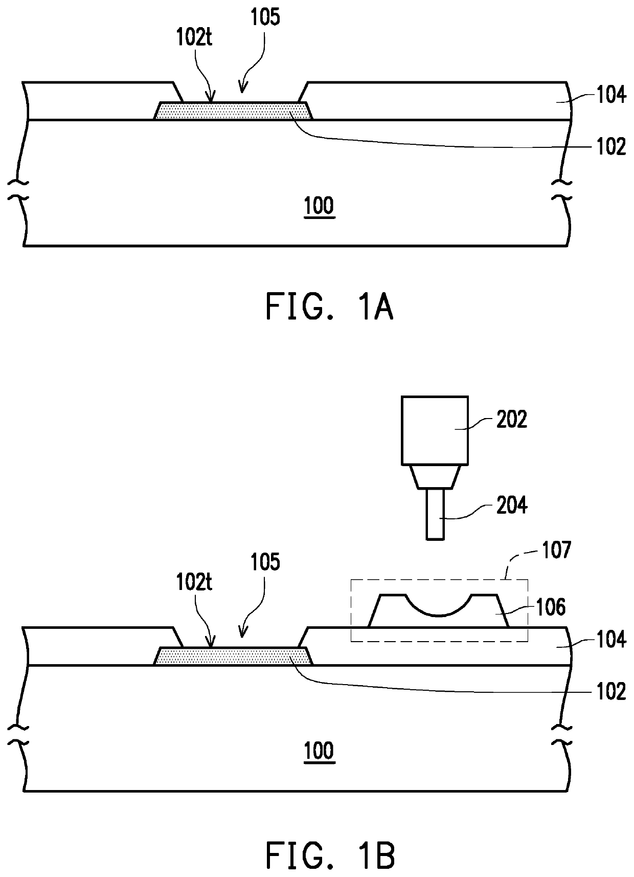
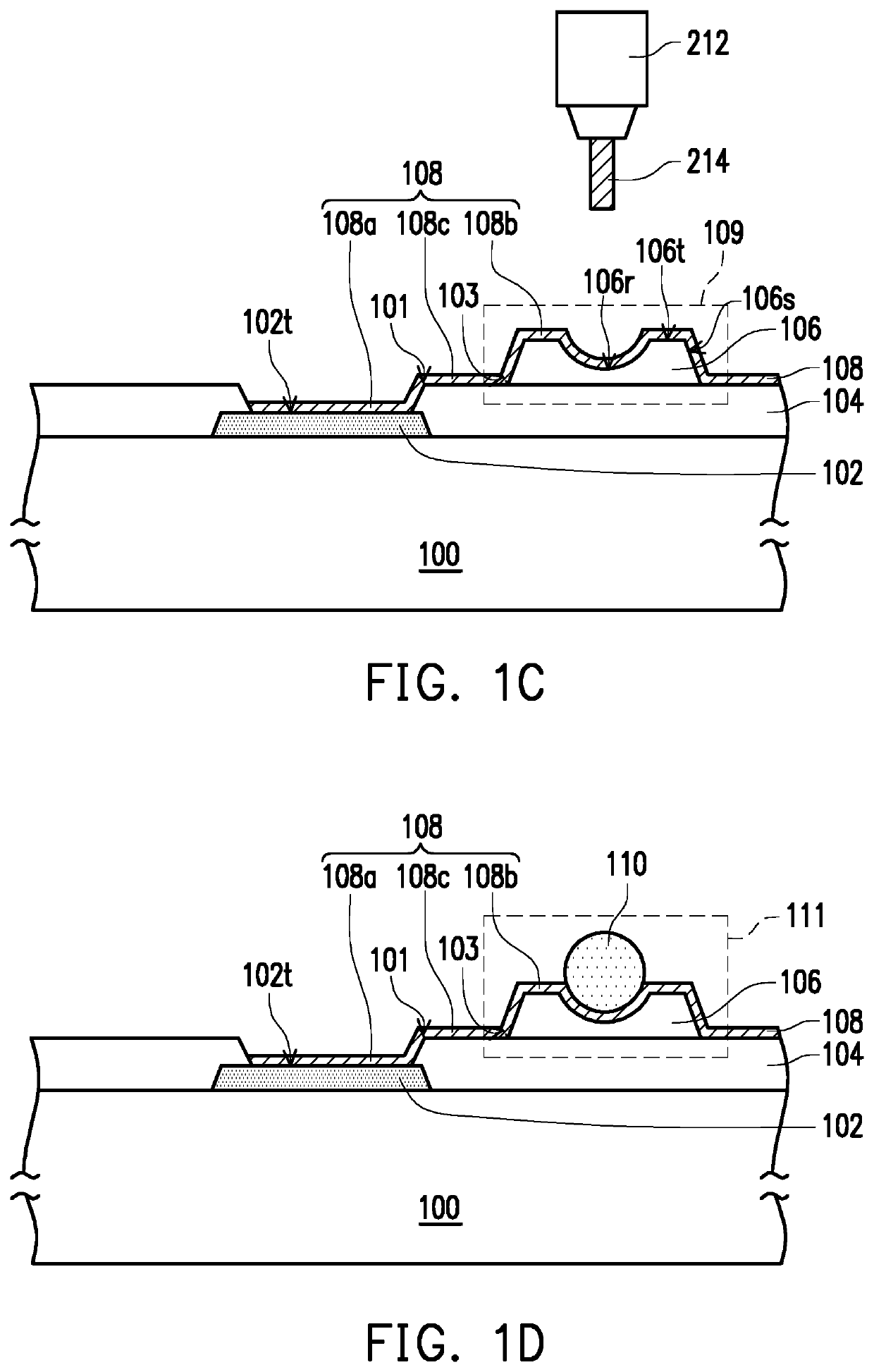
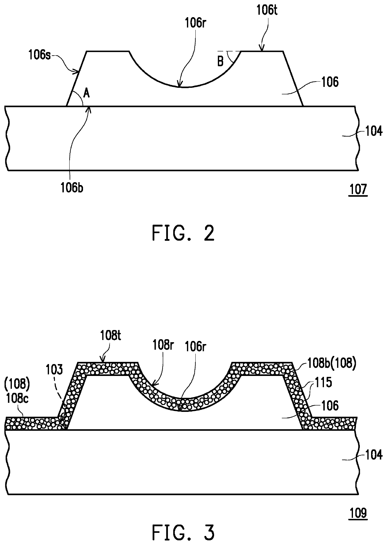
[0015]FIG. 1A to FIG. 1D are schematic cross-sectional views illustrating a manufacturing process of a redistribution layer (RDL) structure according to an embodiment of the disclosure. FIG. 2 is an enlarged cross-sectional view illustrating a portion of the RDL structure depicted in FIG. 1B. FIG. 3 is an enlarged cross-sectional view illustrating a portion of the conductive layer depicted in FIG. 1C. FIG. 4 is an enlarged cross-sectional view illustrating a portion of the RDL s...


PUM

PropertyMeasurementUnit
included angleaaaaaaaaaa
shear angleaaaaaaaaaa

Abstract

Provided is a redistribution layer (RDL) structure including a substrate, a pad, a dielectric layer, a self-aligned structure, a conductive layer, and a conductive connector. The pad is disposed on the substrate. The dielectric layer is disposed on the substrate and exposes a portion of the pad. The self-aligned structure is disposed on the dielectric layer. The conductive layer extends from the pad to conformally cover a surface of the self-aligned structure. The conductive connector is disposed on the self-aligned structure. A method of manufacturing the RDL structure is also provided.

Description

BACKGROUNDTechnical Field[0001]The disclosure relates to a semiconductor structure and a method of manufacturing the same, and more particularly to a redistribution layer (RDL) structure and a method of manufacturing the same.Description of Related Art[0002]Recently, the continuous increase in the integration of various electronic components (e.g., transistors, diodes, resistors, capacitors, and so on) leads to the rapid growth of the semiconductor industry. The increase in the integration mostly results from the continuous reduction of the minimum feature size, so that more components can be integrated into a given area.[0003]Compared to the convention package structure, these electronic components with smaller size occupy smaller area and thus require a smaller package structure. For instance, a semiconductor chip or die has an increasing number of input / output (I / O) solder pads, and a redistribution layer (RDL) can redistribute the original I / O solder pads of the semiconductor ch...

Claims


Application Information

Patent Timeline
Patent Type & Authority Patents(United States)
IPC IPC(8): H01L23/00B22F1/054
CPCH01L24/13H01L24/03H01L24/05H01L24/11H01L2224/024H01L2224/0239H01L2224/02311H01L2224/02373H01L2224/0401H01L2224/13021H01L2224/13024H01L2924/01029H01L2924/01047H01L2924/069H01L2924/07025H01L2224/0236H01L2224/02125H01L2224/02145H01L2224/0215H01L2224/13022H01L2224/03312H01L2224/03505H01L24/02B33Y80/00B29C64/112B33Y10/00B22F7/08B22F10/10B22F2999/00H01L2224/05794H01L2224/13164H01L2224/13124H01L2224/131H01L2224/13139H01L2224/05847H01L2224/13155H01L2224/05839H01L2224/13147H01L2224/13144H01L2224/13111Y02P10/25H01L2224/05548B22F1/054B22F10/22B22F12/53H01L2924/06H01L2924/013H01L2924/00014H01L2924/014B22F1/107
Inventor CHU, YEN-JUIWU, JIN-NENGCHOU, HSIN-HUNGLIN, CHUN-HUNG
Owner WINBOND ELECTRONICS CORP
Why Eureka
Try Eureka