Redistribution layer structure and manufacturing method thereof

A technology for rewiring layers and manufacturing methods, applied in the field of semiconductor structures and their manufacturing, can solve the problems of abnormal solder ball height, small contact area, solder bridging, etc., to improve product reliability, increase contact area, and increase structural strength Effect

Pending Publication Date: 2020-05-29
WINBOND ELECTRONICS CORP
View PDF6 Cites 0 Cited by
  • Summary
  • Abstract
  • Description
  • Claims
  • Application Information

AI Technical Summary

Problems solved by technology

[0004] However, in the traditional wafer-level packaging process, the under-ball metallurgy (UBM) layer has a nearly planar structure, so that the contact area between the UBM layer and the solder ball is small and the bonding force is weak, which leads to the solder ball Delamination or generation of intermetallic compound (IMC) problems
In addition, the abnormal ball height of the solder balls is also likely to cause problems of cold joints or solder bridges during the packaging process.

Method used


Image

  • Redistribution layer structure and manufacturing method thereof
  • Redistribution layer structure and manufacturing method thereof
  • Redistribution layer structure and manufacturing method thereof

Examples


Embodiment Construction

[0013] The present invention will be described more fully with reference to the accompanying drawings of this embodiment. However, the present invention can also be embodied in various forms and should not be limited to the embodiments described herein. In the drawings, the thicknesses of layers and regions may be exaggerated for clarity. The same or similar component numbers represent the same or similar components, and the following paragraphs will not repeat them one by one.

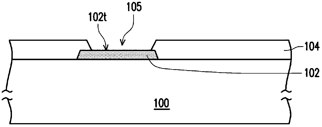
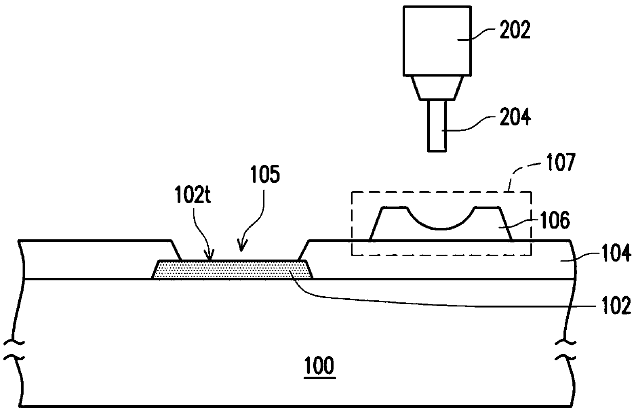
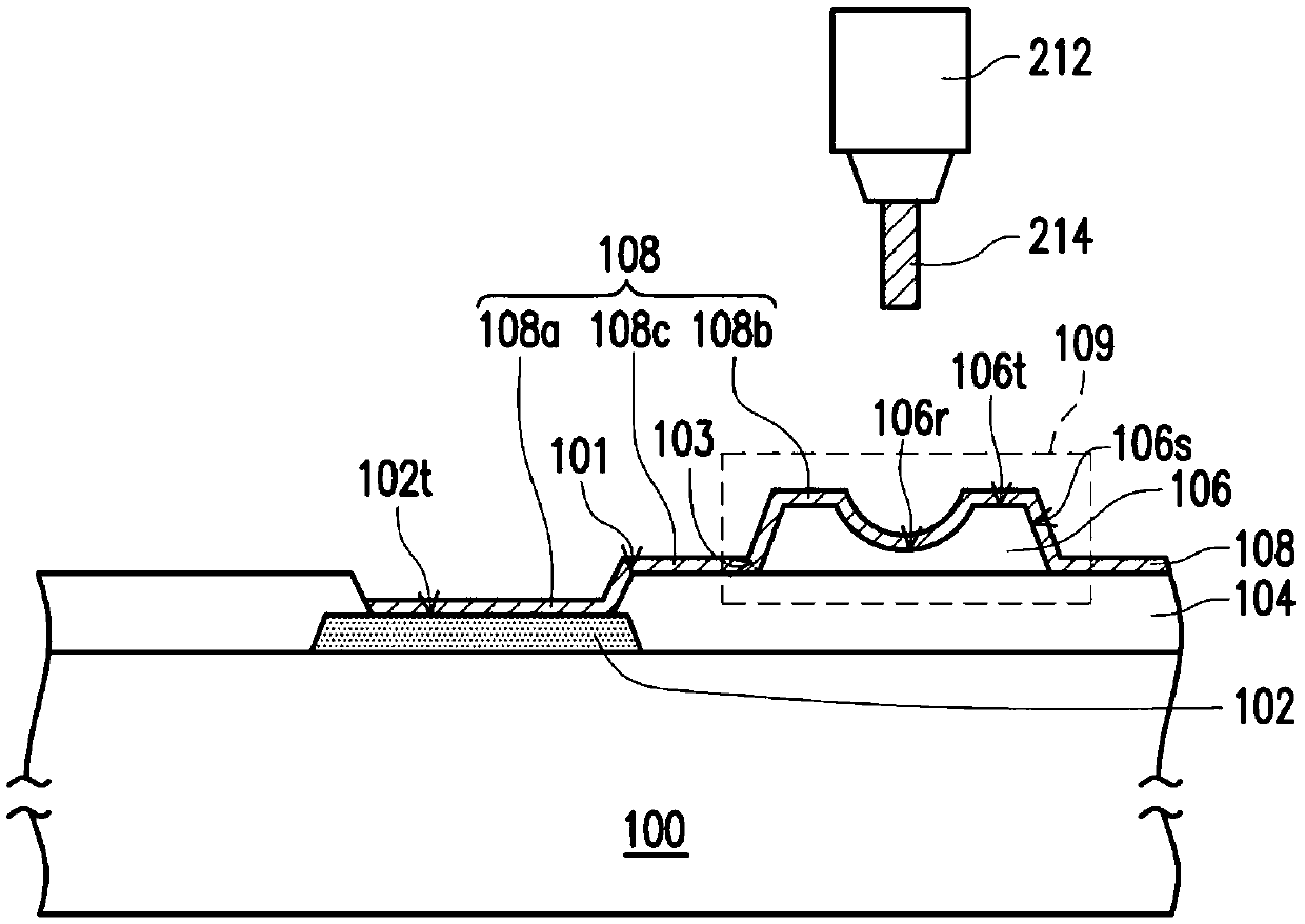
[0014] Figure 1A to Figure 1D is a schematic cross-sectional view of a manufacturing process of a redistribution layer structure according to an embodiment of the present invention. figure 2 yes Figure 1B An enlarged cross-sectional view of a part of the self-aligned structure. image 3 yes Figure 1C An enlarged cross-sectional view of a portion of the conductive layer. Figure 4 yes Figure 1D An enlarged cross-sectional view of a portion of the redistribution layer structure.

[0015] Ple...


PUM

PropertyMeasurementUnit
angleaaaaaaaaaa
thicknessaaaaaaaaaa
particle sizeaaaaaaaaaa

Abstract

The invention provides a redistribution layer structure. The redistribution layer structure comprises a substrate, a connecting pad, a dielectric layer, a self-alignment structure, a conductive layerand a conductive connecting piece; the connecting pad is disposed on the substrate; the dielectric layer is disposed on the substrate and exposes a portion of the connecting pad; the self-alignment structure is disposed on the dielectric layer; the conductive layer extends from the connecting pad and conformally covers the surface of the self-alignment structure; the conductive connecting piece isconfigured on the self-alignment structure. The invention further provides a manufacturing method of the redistribution layer structure.

Description

technical field [0001] The invention relates to a semiconductor structure and a manufacturing method thereof, in particular to a rewiring layer structure and a manufacturing method thereof. Background technique [0002] In recent years, due to the increasing integration of various electronic components (such as transistors, diodes, resistors, capacitors, etc.), the semiconductor industry has grown rapidly. This increase in integration is mostly due to the continuous shrinking of the minimum feature size, allowing more components to be integrated in a specific area. [0003] Compared with conventional packaging structures, these smaller electronic components have smaller areas and thus require smaller packaging structures. For example, a semiconductor chip or die has more and more input / output (I / O) pads, and a redistribution layer (redistribution layer, RDL) can replace the original I / O pads of the semiconductor chip or die. Locations are relocated around the semiconductor...

Claims


Application Information

Patent Timeline
Patent Type & Authority Applications(China)
IPC IPC(8): H01L23/488H01L21/60
CPCH01L24/02H01L24/13H01L2021/60075H01L2224/02319H01L2224/0235H01L2224/13021H01L2224/023H01L2224/11H01L2224/13H01L2924/0001
Inventor 朱彦瑞吴金能周信宏林俊宏
Owner WINBOND ELECTRONICS CORP
Why Eureka
Try Eureka