Thermal fluid flow sensor

a technology of thermal fluid flow and sensor, which is applied in the manufacture/treatment of thermoelectric devices, instruments, liquid/fluent solid measurements, etc., can solve the problems of low sensitivity, slow dynamic response of the sensor, and high power dissipation, so as to reduce the size and cost of the sensor, increase the sensitivity of the sensor, and reduce the thermal conductivity of the membrane stack

Active Publication Date: 2021-07-20
CAMBRIDGE GAN DEVICES LIMITED
View PDF25 Cites 6 Cited by
  • Summary
  • Abstract
  • Description
  • Claims
  • Application Information

AI Technical Summary

Benefits of technology

[0015](i) Enhanced thermal isolation, while maintaining robustness, through the membrane structure for low power consumption, high sensitivity and fast response
[0114]The nucleation layer (which may be formed on AlN) may be used as an etch stop during the DRIE or wet etching processes. Subsequently the AlN nucleation layer may be removed during etching, to lower the thermal conductivity of the membrane stack and increase the sensitivity of the sensor.

Problems solved by technology

The main drawback of all the previously mentioned citations resides in the lack of an effective thermal isolation of the heated element, which results in high power dissipation, low sensitivity, and slow dynamic response of the sensor.
The issue associated with the use of a cantilever structure is that they suffer from mechanical fragility and vibration sensitivity.
The use of polyimide, although improving the beam thermal isolation, further affects the mechanical robustness of the beam.
The use of silicon as membrane material is not ideal due to the high thermal conductivity of the silicon layer.
This results in high power dissipation, low sensitivity and slow dynamic response of the sensor.
However, the thermocouples still provide an additional thermal dissipation path within the membrane, thus increasing the power dissipation, lowering the sensitivity and slowing down the dynamic response of the sensor.
However, gold is used and this make the process not fully CMOS compatible, and thus more expensive than a fully CMOS process.
Nickel is not a standard CMOS material, making the sensor fabrication process more expensive than a fully CMOS process.
The 2D carrier gas is extremely susceptible to external chemical stimuli.
Injection of a current into the 2D carrier device formed within the membrane results in a localised increase in temperature.
Injection of a current into the resistive heating element results in a localised increase in temperature.

Method used


Image

  • Thermal fluid flow sensor
  • Thermal fluid flow sensor
  • Thermal fluid flow sensor

Examples


Embodiment Construction

[0118]Some preferred embodiments of the disclosure will now be described by way of example only and with reference to the accompanying drawings, in which:

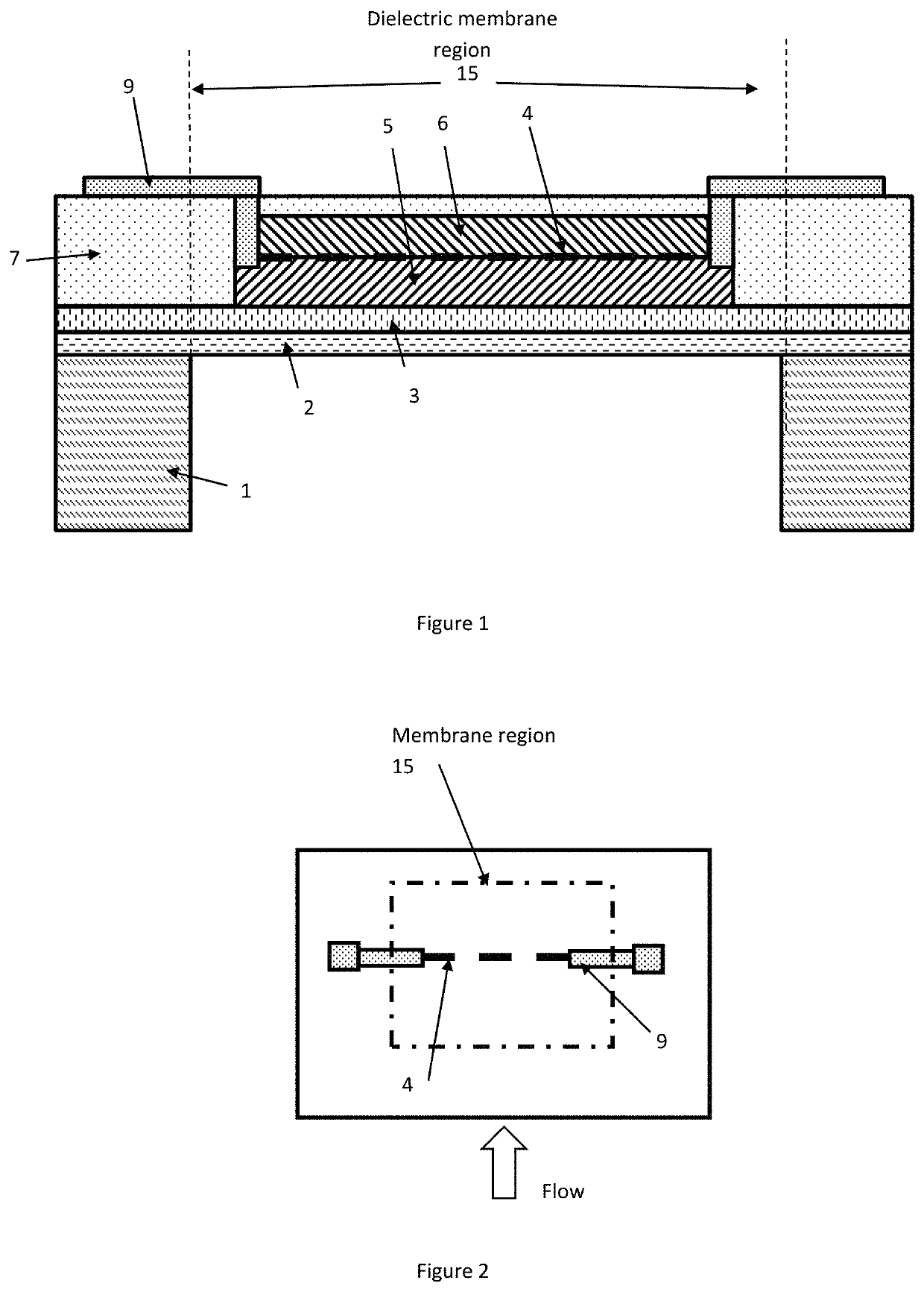
[0119]FIG. 1 shows a cross section of a heterostructure based sensor;

[0120]FIG. 2 shows a top view of a heterostructure based sensor;

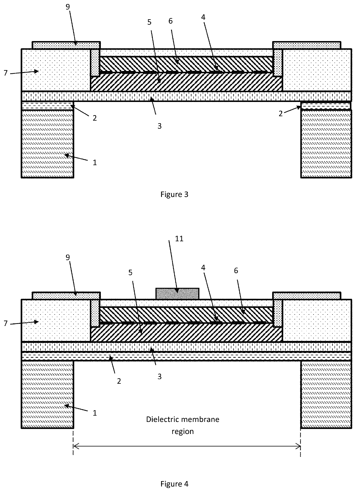
[0121]FIG. 3 shows a cross section of a heterostructure based sensor. The nucleation layer has been etched;

[0122]FIG. 4 shows a cross section of a heterostructure based sensor. An additional gate is formed on the sensor;

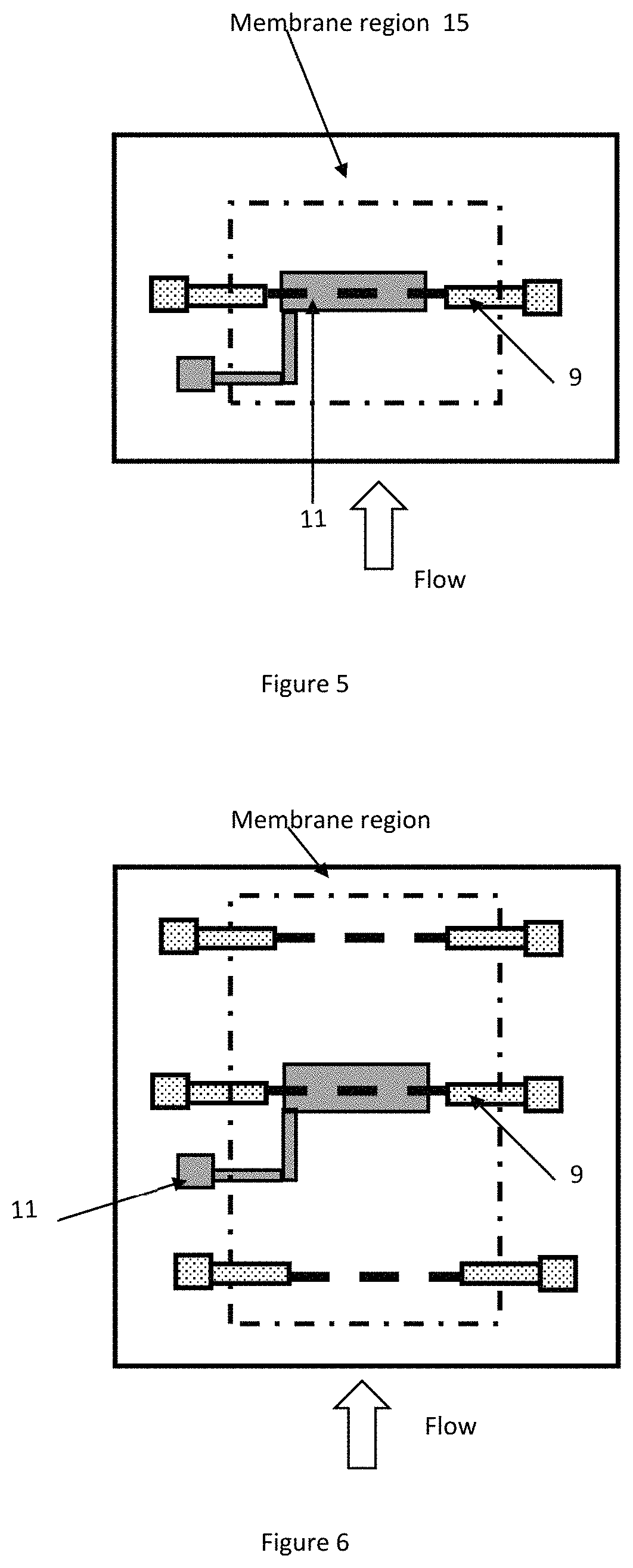
[0123]FIG. 5 shows a top view of a heterostructure based sensor. An additional gate is formed on the sensor;

[0124]FIG. 6 shows a top view of a heterostructure based sensor. Three elements are formed on the membrane region;

[0125]FIG. 7 shows a cross section of a heterostructure based sensor. An ASIC is assembled at the bottom of the sensor for stack-assembly in the same package;

[0126]FIG. 8 shows a cross section of a heterostructure-based infra-red device that can be operated as IR emit...


PUM

PropertyMeasurementUnit
temperatureaaaaaaaaaa
areaaaaaaaaaaa
band gapaaaaaaaaaa

Abstract

We disclose herewith a heterostructure-based sensor comprising a substrate comprising an etched portion and a substrate portion; a device region located on the etched portion and the substrate portion; the device region comprising at least one membrane region which is an area over the etched portion of the substrate. At least one heterostructure-based element is located at least partially within or on the at least one membrane region, the heterostructure-based element comprising at least one two dimensional (2D) carrier gas.

Description

RELATED APPLICATION DATA[0001]This application is a continuation-in-part (CIP) of U.S. patent application Ser. No. 15 / 938,425, filed Mar. 28, 2018, the disclosure of which is incorporated herein by reference in its entirety.FIELD OF THE INVENTION[0002]This disclosure relates to a micro-machined sensor. Particularly, but not exclusively, this disclosure relates to a hetero-structure based thermal fluid flow sensor.BACKGROUND OF THE INVENTION[0003]Thermal fluid flow sensors rely on the thermal interaction between the sensor itself and the fluid. Depending upon the physical phenomena governing the interaction, flow sensors can be can be classified into the following three categories: (i) anemometric sensors measure the convective heat transfer induced by fluid flow passing over a heated element; (ii) calorimetric sensors detect the asymmetry of the temperature profile generated by a heated element and caused by the forced convection of the fluid flow; (iii) time of flight (ToF) sensors...

Claims


Application Information

Patent Timeline
Patent Type & Authority Patents(United States)
IPC IPC(8): G01F1/688G01F1/698G01L9/00H01L35/34H01L35/30H01L35/22H01L35/32
CPCG01F1/6888G01F1/698G01L9/008H01L35/34H01L35/22H01L35/30H01L35/32H10N10/855H10N10/01H10N10/17H10N10/13
Inventor UDREA, FLORINDE LUCA, ANDREALONGOBARDI, GIORGIA
Owner CAMBRIDGE GAN DEVICES LIMITED
Why Eureka
Try Eureka