Radiation detector and compton camera

a technology of radiometer and camera, applied in the field of radiometer, can solve the problem that the device cannot specify the incident time and energy of the radiation from the transferred image signal

Active Publication Date: 2021-09-07
CANON KK
View PDF11 Cites 0 Cited by
  • Summary
  • Abstract
  • Description
  • Claims
  • Application Information

AI Technical Summary

Problems solved by technology

However, the time when the transferred charges are accumulated cannot be specified, so that a reading time period of the image signals becomes a dead time period and an incident time from a radiation source cannot be specified.
Thus, the existing radiation detector using the charge-accumulation two-dimensional semiconductor device cannot specify the incident time and energy of the radiation from the transferred image signals.

Method used


Image

  • Radiation detector and compton camera
  • Radiation detector and compton camera
  • Radiation detector and compton camera

Examples


Embodiment Construction

[0016]While an X-ray is used as an example of radiation in exemplary embodiments, some embodiments are applicable to a gamma ray.

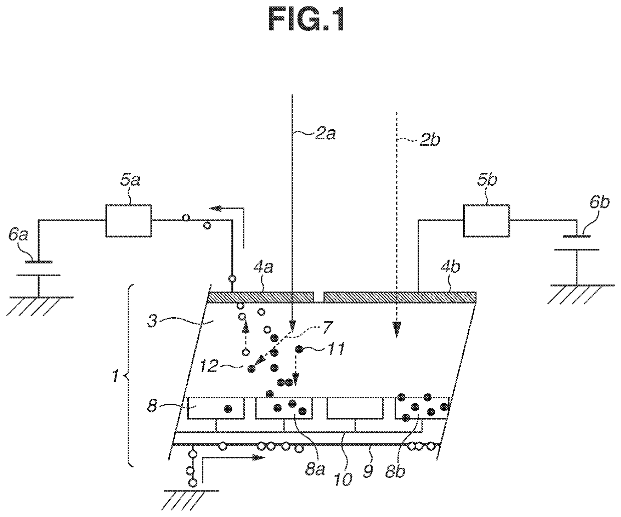
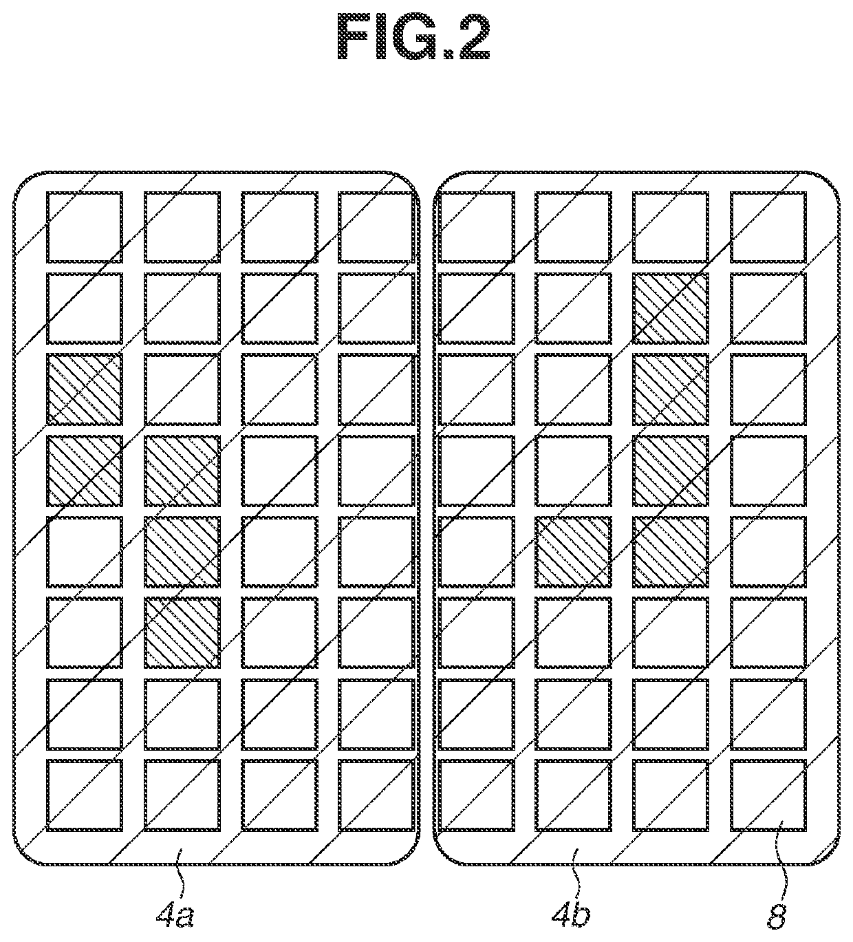
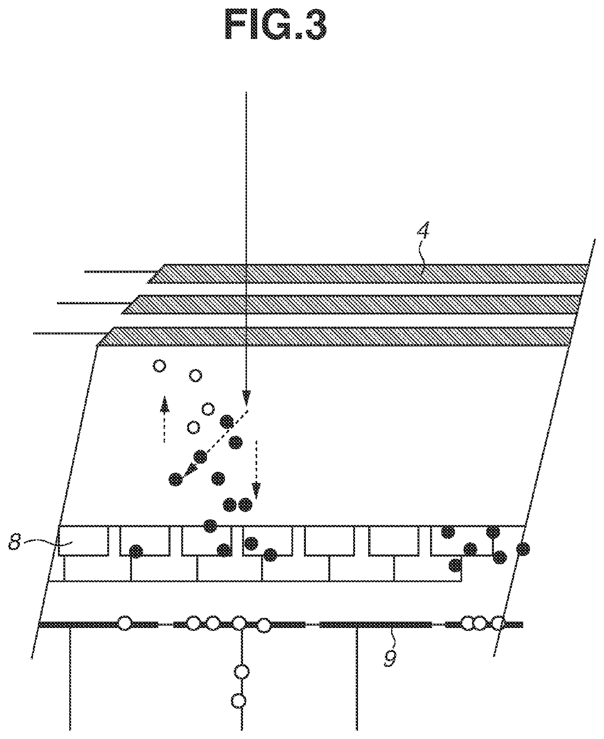
[0017]A first exemplary embodiment will be described below. Referring to FIG. 1, which is a partial sectional view of an X-ray detector 1 according to an embodiment, the X-ray detector 1 includes a semiconductor substrate 3 that is a layer that is sensitive to an X-ray, as illustrated by X-rays 2 (2a and 2b) in FIG. 1, and front-surface electrodes 4a and 4b (both may collectively referred to as front-surface electrode 4) and a back-surface electrode 9 formed on front and back surfaces of the semiconductor substrate 3, respectively. The plurality of front-surface electrodes 4a and 4b is provided on the surface of the semiconductor substrate 3 on which an X-ray is incident (radiation incident side). The X-ray detector 1 is a two-dimensional semiconductor device using a silicon (Si) substrate, such as a complementary metal-oxide semiconductor (CMOS) and a cha...


PUM

PropertyMeasurementUnit
charge accumulationaaaaaaaaaa
timeaaaaaaaaaa
voltageaaaaaaaaaa

Abstract

The present disclosure concerns a charge-accumulation radiation detector that includes a semiconductor device and specifies an incident time and energy of radiation from a transferred image signal. The radiation detector includes a semiconductor substrate and electrodes disposed on both sides of the semiconductor substrate, and includes a plurality of charge accumulation units inside the semiconductor substrate. The plurality of charge accumulation units is each configured to accumulate charges generated by radiation incident on the semiconductor substrate. The charges accumulated in the charge accumulation units are readable to outside through at least one of the electrodes.

Description

BACKGROUNDField of the Disclosure[0001]The present disclosure relates to a radiation detector that detects radiation as an observation target by detecting photoelectrons generated by a photoelectric effect and recoil electrons generated by Compton scattering, and to a Compton camera.Description of the Related Art[0002]Radiation detection apparatuses using a semiconductor device have been available. Japanese Patent Application Laid-Open No. 2014-185852 discusses a radiation detection apparatus including first and second detection units. The first detection unit detects a position at which a first interaction occurs due to incident radiation and a track of a recoil electron generated by the first interaction, with use of a first photoelectric conversion device. The second detection unit detects a position at which a second interaction occurs due to scattered radiation. A position of a radiation source in an observation target space is calculated with use of the positions at which the ...

Claims


Application Information

Patent Timeline
Patent Type & Authority Patents(United States)
IPC IPC(8): G01T1/24G01T1/29G01T1/20
CPCG01T1/241G01T1/20G01T1/247G01T1/2928G01T1/17
Inventor AMEMIYA, MITSUAKI
Owner CANON KK
Why Eureka
Try Eureka