Imaging optical system, camera module, and electronic device

a technology of optical system and electronic device, applied in the field of imaging optical system, camera module, electronic device, can solve the problems of reducing peripheral light amount, pixel pitch becoming extremely small in the solid-state imaging element, and reducing the amount of ligh

Active Publication Date: 2021-10-26
SONY SEMICON SOLUTIONS CORP
View PDF14 Cites 0 Cited by
  • Summary
  • Abstract
  • Description
  • Claims
  • Application Information

AI Technical Summary

Benefits of technology

[0017]In the imaging optical system, the camera module, or the electronic device according to the present disclosure, the light transmittance value at least in a peripheral portion of the optical member is larger than the light transmittance value in the central portion. Accordingly, nonuniformity of the light amount due to the decrease in light amount at the peripheral portion (edge portion) of the screen is optically corrected by the optical member. That is, according to the present disclosure, it is possible to optically correct the nonuniformity of the light amount due to the decrease in the peripheral light amount based on the optical characteristics of the lens by using the imaging optical system, rather than by correction in signal processing. Note that effects described herein are non-limiting. The effects may be any effects described in the present description. In addition, effects described herein are provided for purposes of exemplary illustration and are not intended to be limiting. Still other additional effects may also be contemplated.

Problems solved by technology

Furthermore, with this trend of using highly miniaturized cameras with higher pixel resolution, pixel pitch is becoming extremely small in a solid-state imaging element such as a CCD image sensor or a CMOS image sensor mounted on an imaging apparatus.
Under such circumstances, there is a problem of small aperture diffraction in a lens of an imaging optical system that captures image light (incident light) from a subject and guides the light to an imaging surface of a solid-state imaging element.
However, it is known that increasing aperture of the lens would induce another problem of reduction in the peripheral light amount (vignetting), that is, the amount of light decreases at peripheral portions (edge portions) of the screen, caused by optical characteristics of the lens.
However, the amplification processing in the signal processing system of the solid-state imaging element has problems of emphasized noise component, emphasized flaw in the solid-state imaging element, emphasized fine dust attached to the solid-state imaging element, emphasized unevenness of the solid-state imaging element or optical materials and the like, and these problems lead to reduction in the yield of the imaging apparatus.

Method used


Image

  • Imaging optical system, camera module, and electronic device
  • Imaging optical system, camera module, and electronic device
  • Imaging optical system, camera module, and electronic device

Examples


first embodiment

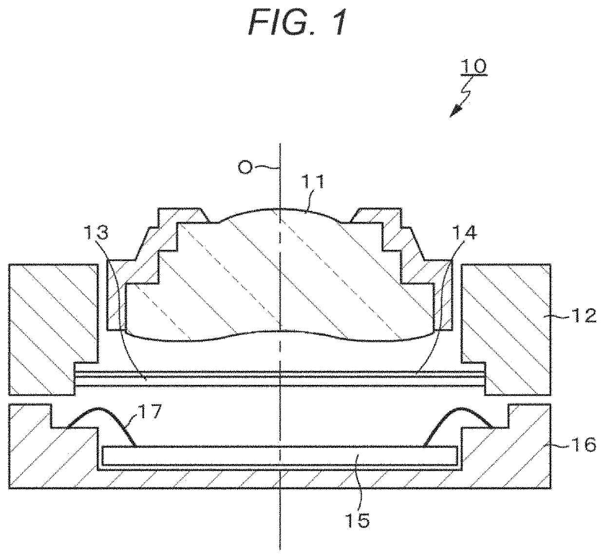
[0049]The first embodiment of the present disclosure is an example of mounting a solid-state imaging element on a circuit substrate. FIG. 1 illustrates a cross-sectional structure of a camera module according to the first embodiment. The camera module according to the first embodiment includes an imaging optical system according to the present disclosure.

[0050]As illustrated in FIG. 1, the imaging optical system according to the first embodiment includes a lens (condenser lens 11) and an optical member (specifically, an ND filter 14), and the camera module 10 includes this imaging optical system. Specifically, the camera module 10 according to the first embodiment includes a condenser lens 11, a lens driving unit 12, an infrared cut filter (hereinafter referred to as “IR cut filter”) 13, and the ND filter 14. The camera module 10 further includes a solid-state imaging element 15, a circuit substrate 16, and a metal wire 17.

[0051]In the camera module 10 having the above-described con...

second embodiment

[0067]A second embodiment of the present disclosure is an example of accommodating a solid-state imaging element in a package. FIG. 7 illustrates a cross-sectional structure of an imaging optical system according to the second embodiment. Similarly to the camera module according to the first embodiment, a camera module according to the second embodiment also includes the imaging optical system according to the present disclosure.

[0068]The camera module 10 according to the second embodiment differs, in configuration, from the camera module 10 according to the first embodiment having the solid-state imaging element 15 mounted on the circuit substrate 16, in that the solid-state imaging element 15 is packaged (accommodated) in a package 18 including a light-transmissive material. For the other configurations, the camera module 10 of the second embodiment is basically the same as the camera module 10 of the first embodiment. Accordingly, in the imaging optical system, the ND filter 14 p...


PUM

PropertyMeasurementUnit
sizeaaaaaaaaaa
light transmittanceaaaaaaaaaa
opticalaaaaaaaaaa

Abstract

An imaging optical system according to the present disclosure includes: a lens; and an optical member, in which the optical member is configured such that a light transmittance value at least in a peripheral portion is larger than a light transmittance value in a central portion. Furthermore, a camera module according to the present disclosure includes the imaging optical system of the present disclosure. Furthermore, an electronic device according to the present disclosure includes a solid-state imaging element and the imaging optical system of the present disclosure.

Description

CROSS REFERENCE TO RELATED APPLICATIONS[0001]This application is a U.S. National Phase of International Patent Application No. PCT / JP2017 / 040287 filed on Nov. 8, 2017, which claims priority benefit of Japanese Patent Application No. JP 2016-230962 filed in the Japan Patent Office on Nov. 29, 2016. Each of the above-referenced applications is hereby incorporated herein by reference in its entirety.TECHNICAL FIELD[0002]The present disclosure relates to an imaging optical system, a camera module, and an electronic device.BACKGROUND ART[0003]Recently, in imaging apparatuses such as a digital still camera and a mobile terminal apparatus with a camera, there is a trend of using a highly miniaturized camera with higher pixel resolution (with larger number of pixels). Furthermore, with this trend of using highly miniaturized cameras with higher pixel resolution, pixel pitch is becoming extremely small in a solid-state imaging element such as a CCD image sensor or a CMOS image sensor mounted...

Claims


Application Information

Patent Timeline
Patent Type & Authority Patents(United States)
IPC IPC(8): G02B5/20H04N5/225H04N5/372G02B9/04G02B5/00G02B9/02
CPCG02B5/205G02B5/00G02B5/208G02B9/02G02B9/04H04N5/225H04N5/2254H04N5/372G02B7/08G02B23/2476G02B23/2461G02B23/2446A61B1/042A61B1/00188A61B1/00165A61B1/00149A61B1/00193A61B1/07A61B1/0684A61B1/043A61B1/045A61B1/002A61B1/00006G02B27/58A61B1/0004A61B1/000095A61B1/0655H04N23/55H04N23/00H04N25/71
Inventor KIMURA, KATSUJI
Owner SONY SEMICON SOLUTIONS CORP
Why Eureka
Try Eureka