Adjustable capacitor, impedance matching device and semiconductor processing apparatus

a technology of impedance matching and adjustment capacitor, which is applied in the field of microelectronic processing, can solve the problems of difficult to achieve a matching speed in a millisecond order, and achieve the effect of increasing the adjustment rate of the capacitance value, shortening the adjustment time, and rapid change of the capacitan

Active Publication Date: 2021-11-30
BEIJING NAURA MICROELECTRONICS EQUIP CO LTD
View PDF9 Cites 0 Cited by
  • Summary
  • Abstract
  • Description
  • Claims
  • Application Information

AI Technical Summary

Benefits of technology

[0007]The present disclosure aims to solve at least one of the technical problems in the existing technologies, and provides an adjustable capacitor and an impedance matching device, which can adjust the capacitance of the adjustable capacitor in milliseconds or less, thereby achieving the matching speed in milliseconds or less.
[0021]The adjustable capacitor provided by the embodiment of the present disclosure can control the strength of the electric field where the ferroelectric dielectric layer is disposed by controlling the voltage between the first control electrode and the second control electrode; a rapid change of the electric field strength can cause a rapid change of the dielectric constant of the ferroelectric dielectric layer, the rapid change of the dielectric constant can cause a rapid change of the capacitance between the first electrode and the second electrode, and therefore, compared to the existing mechanical adjustment method, the present disclosure can increase the adjustment rate of the capacitance value and shorten the adjustment time, to achieve adjusting the capacitor in a time period of milliseconds or less.
[0022]The impedance matching device provided by the embodiment of the present disclosure can achieve a matching speed of milliseconds by employing the adjustable capacitor provided by the embodiment of the present disclosure.
[0023]The semiconductor processing apparatus provided by the embodiment of the present disclosure can achieve fast matching between the output impedance of the RF power source and the load impedance by employing the impedance matching device provided by the embodiment of the present disclosure, thereby improving the processing efficiency and the processed result.

Problems solved by technology

However, the use of the impedance matching device as shown in FIG. 1 may inevitably cause the following problems in practical applications: the impedance matching device shown in FIG. 1 changes the capacitance of the capacitor by the rotation of the motor, and the impedance matching speed is affected by the rotational speed of the motor, which results in the matching speed usually in a second order, and would be difficult to achieve a matching speed in a millisecond order.

Method used


Image

  • Adjustable capacitor, impedance matching device and semiconductor processing apparatus
  • Adjustable capacitor, impedance matching device and semiconductor processing apparatus
  • Adjustable capacitor, impedance matching device and semiconductor processing apparatus

Examples


embodiment one

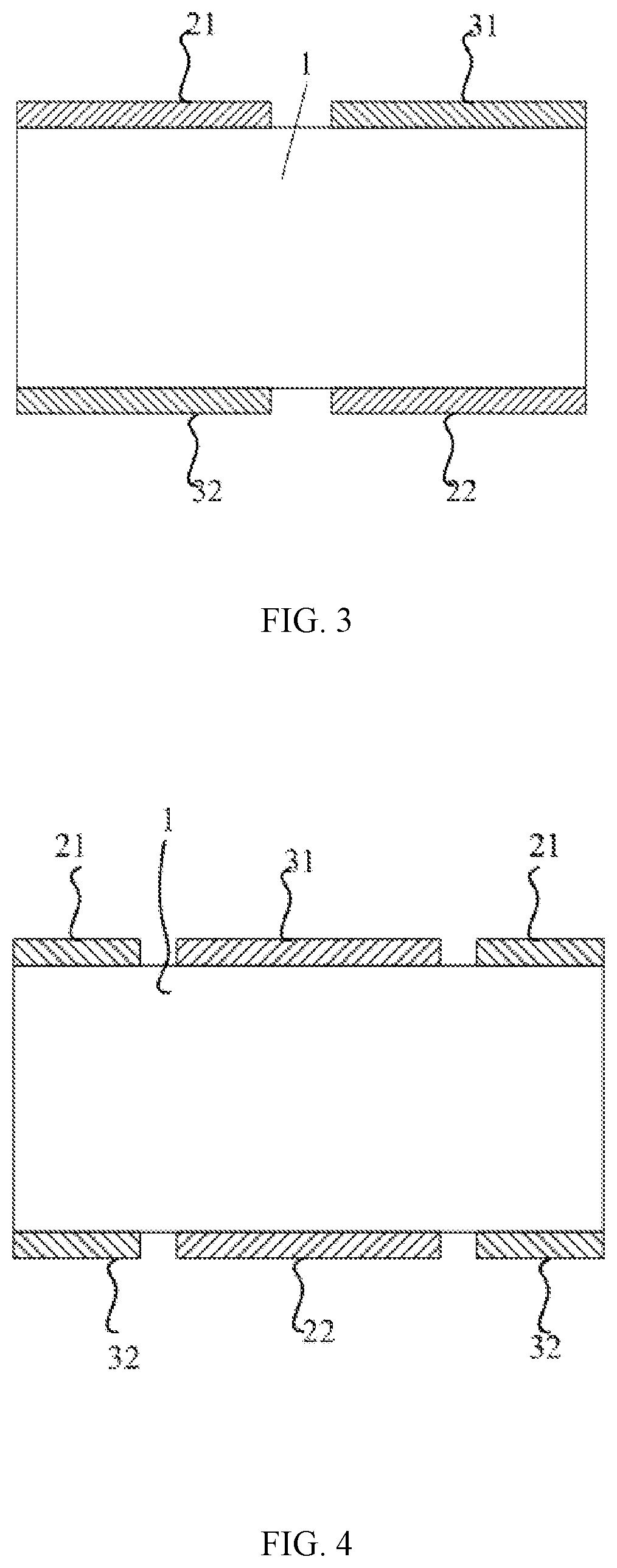
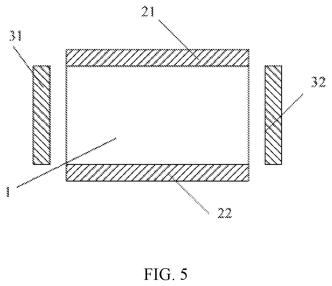
[0032]The current embodiment of the present disclosure provides an adjustable capacitor, the adjustable capacitor includes: a ferroelectric dielectric layer, and a first electrode and a second electrode disposed on opposite sides of the ferroelectric dielectric layer; the adjustable capacitor further includes a first control electrode and a second control electrode insulated from the first electrode and the second electrode; the first control electrode and the second control electrode are configured to provide an electric field to the ferroelectric dielectric layer to adjust a dielectric constant of the ferroelectric dielectric layer by controlling an electric field strength, thereby adjusting a capacitance of a capacitor between the first electrode and the second electrode. That is to say, the first electrode and the second electrode are two electrodes of the adjustable capacitor provided by the embodiment of the present disclosure, and the first control electrode and the second co...

embodiment two

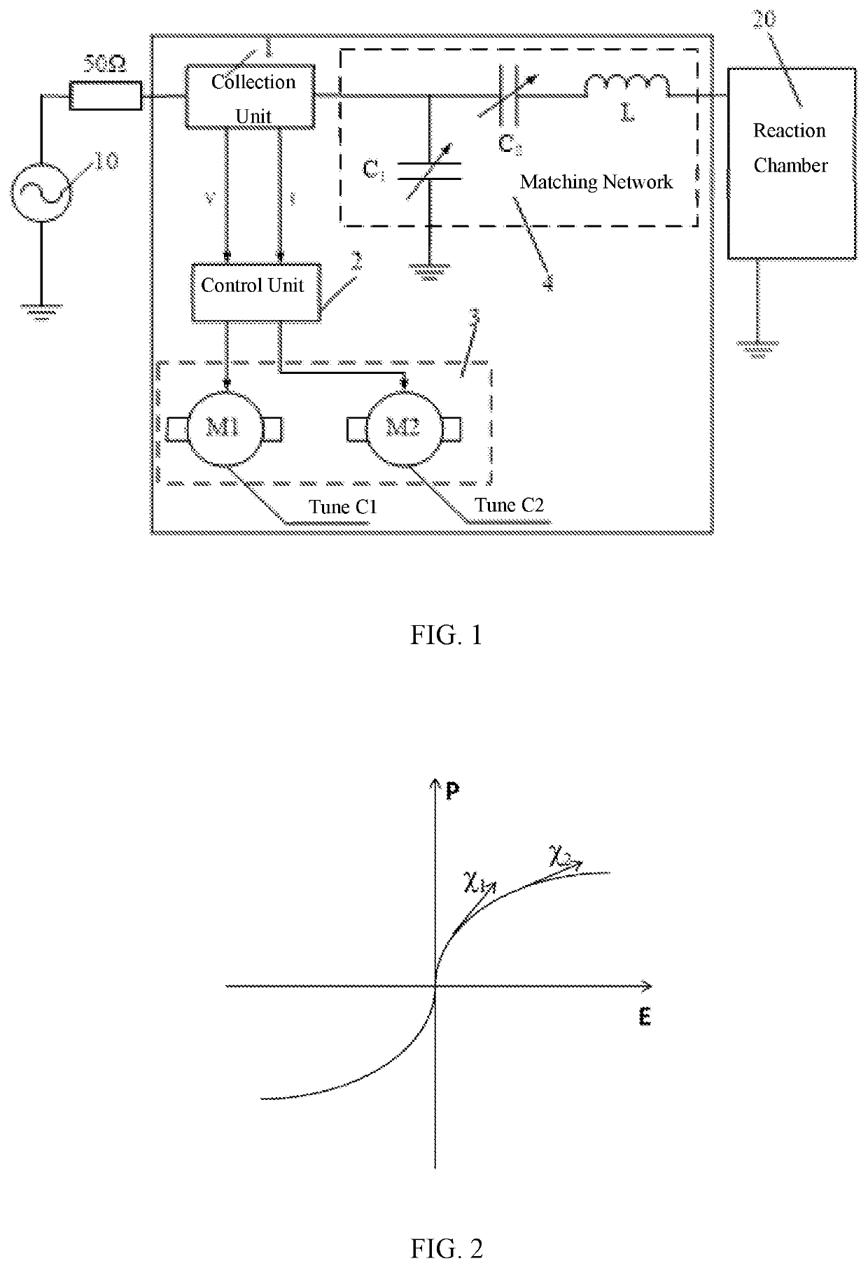
[0046]The present embodiment provides an impedance matching device. As shown in FIG. 6, the impedance matching device includes a matching network 50, an collection unit 51, and a control unit 52. The matching network 50 includes the adjustable capacitor provided in the above Embodiment One, the electrode 21 and the second electrode 22 are connected to the circuit of the matching network 50. The first control electrode 31 is electrically connected to the control unit 52, and the second control electrode 32 is grounded.

[0047]The matching network 50 is connected in series between the RF power source 10 and the reaction chamber 20; the collection unit 51 is configured to collect electrical signals in the transmission line between the RF power source 10 and the matching network 50, and send the electrical signals to the control unit 52; The control unit 52 is configured to perform an impedance matching operation according to the electrical signals collected by the collection unit 51, and...

embodiment three

[0055]The present embodiment provides a semiconductor processing apparatus. As shown in FIG. 7, the semiconductor processing apparatus includes an RF power source 10, an impedance matching device 60, and a reaction chamber 20; the impedance matching device 60 is connected in series between the RF power source 10 and the reaction chamber 20, configured to match the output impedance of the RF power source with the load impedance. The impedance matching device 60 employs the impedance matching device provided in the above Embodiment Two.

[0056]The semiconductor processing apparatus in this embodiment employs the impedance matching device provided in the Embodiment Two, to achieve fast matching between the output impedance of the RF power source and the load impedance, thereby improving processing efficiency and processed result.


PUM

PropertyMeasurementUnit
output impedanceaaaaaaaaaa
ferroelectricaaaaaaaaaa
electric fieldaaaaaaaaaa

Abstract

The present disclosure provides an adjustable capacitor comprising a ferroelectric dielectric layer, a first electrode and a second electrode disposed on opposite sides of the ferroelectric dielectric layer. The adjustable capacitor further comprises a first control electrode and a second control electrode insulated from the first electrode and the second electrode. The first control electrode and the second control electrode are configured to provide an electric field to the ferroelectric dielectric layer, to adjust a dielectric constant of the ferroelectric dielectric layer by controlling an electric field strength, thereby adjusting the capacitance between the first and the second electrodes. The present disclosure also provides an impedance matching device and a semiconductor processing apparatus. The adjustable capacitor, the impedance matching device and the semiconductor processing apparatus can adjust the capacitance of the adjustable capacitor in milliseconds, thereby accelerating the matching speed, shortening the matching time, and improving the processed result.

Description

[0001]This application is a National Stage entry under § 371 of International Application No. PCT / CN2017 / 106668, filed on Oct. 18, 2017, and claims priority to Chinese Patent Application No. 201710485860.2, filed on Jun. 23, 2017, the entire contents of which are hereby incorporated as reference.TECHNICAL FIELD[0002]The present disclosure relates to the technical field of microelectronic processing, and in particular relates to an adjustable capacitor, an impedance matching device and a semiconductor processing apparatus.BACKGROUND TECHNOLOGY[0003]Plasma technology is widely used in the technical field of semiconductor manufacturing. In a plasma deposition and etching system, an RF power source is used to transmit energy to a reaction chamber to excite a processing gas in the chamber to form a plasma. The plasma contains a large amount of active particles, such as electrons, ions, excited atoms, molecules, and radicals. These active particles can have various physical and chemical r...

Claims


Application Information

Patent Timeline
Patent Type & Authority Patents(United States)
IPC IPC(8): H01J37/32H01G7/06H01L21/67H03H7/42
CPCH01J37/32183H01G7/06H01L21/67069H03H7/42H05H1/46H05H1/4645H03H7/40H01G5/011H01L21/67005
Inventor WEI, GANGCHENG, XIAOYANG
Owner BEIJING NAURA MICROELECTRONICS EQUIP CO LTD
Why Eureka
Try Eureka