Array substrate and flexible display panel
a flexible display panel and array substrate technology, applied in the field of array substrates, can solve the problems of ineffective subpixels, ineffective subpixels, and ineffective subpixels, and achieve the effect of increasing the density of spacers in distribution, effectively avoiding subpixel failure, and prolonging the service life of array substrates
- Summary
- Abstract
- Description
- Claims
- Application Information
AI Technical Summary
Benefits of technology
Problems solved by technology
Method used
Image
Examples
embodiment 1
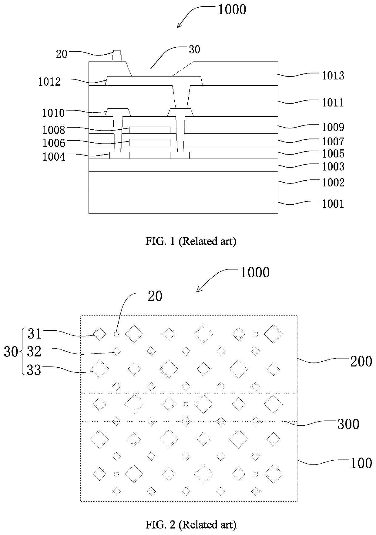
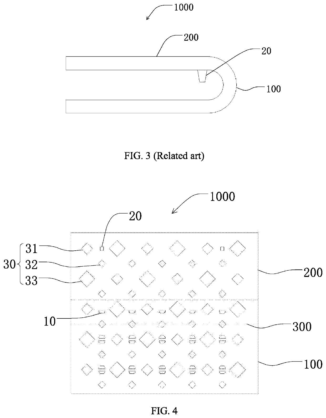
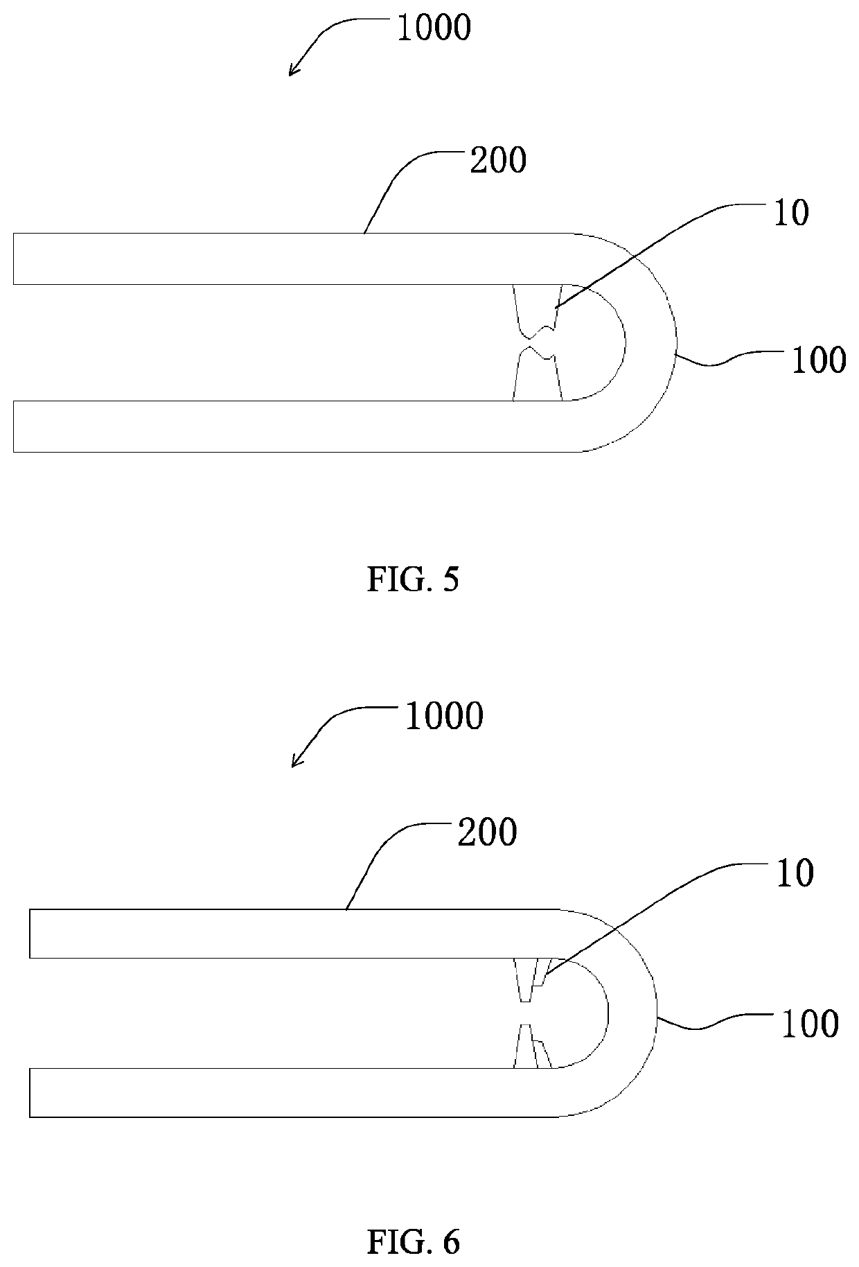
[0032]As illustrated in FIG. 4, an array substrate 1000 is proposed by a first embodiment of the present disclosure. The array substrate 1000 includes a bending area 100 and a non-bending area 200. The bending area 100 is connected to the non-bending area 200. A bending centerline 300 is disposed on the bending area 100. When the array substrate 1000 is arranged flat, the width of the bending area 100 is 2π (times the bending radius. In another embodiment, the width of a bending area 100 is 20 millimeters (mm), which is not specifically limited. Those skilled in the art can decide in reality.
[0033]The array substrate 1000 further includes a plurality of subpixels 30, a plurality of first spacers 10, and a plurality of second spacers 20.
[0034]The array of subpixels 30 is distributed over a bending area 100 and a non-bending area 200. The subpixel 30 includes a red subpixel 31, a blue subpixel 32, and a green subpixel 33. The red subpixel 30 and the blue subpixel 32 are arranged in a ...
embodiment 2
[0041]As illustrated in FIG. 4, an array substrate 1000 is proposed by a second embodiment of the present disclosure. The array substrate 1000 includes a bending area 100 and a non-bending area 200. The bending area 100 is connected to the non-bending area 200. A bending centerline 300 is disposed on the bending area 100. When the array substrate 1000 is arranged flat, the width of the bending area 100 is 2π times the bending radius. In another embodiment, the width of a bending area 100 is 20 millimeters (mm), but is not specifically limited. Those skilled in the art can decide according to actual needs.
[0042]Further, the array substrate 1000 includes a plurality of subpixels 30, a plurality of first spacers 10, and a plurality of second spacers 20.
[0043]The array of subpixels 30 is distributed over a bending area 100 and a non-bending area 200. The subpixel 30 includes a red subpixel 31, a blue subpixel 32, and a green subpixel 33. The red subpixel 30 and the blue subpixel 32 are ...
PUM
 Abstract
Description
Claims
Application Information


