Electron emission element and method for manufacturing same

a technology of electron emission element and manufacturing method, which is applied in the manufacture of electric discharge tubes/lamps, discharge tube cold cathodes, and discharge tube coatings. it can solve the problems of reducing sudden breakdown so as to prolong the life of the electron emission element, reduce the effect of sudden breakdown of the element, and use the effect of an electron emission surface uniformly

Active Publication Date: 2021-12-21
SHARP KK
View PDF2 Cites 0 Cited by
  • Summary
  • Abstract
  • Description
  • Claims
  • Application Information

AI Technical Summary

Benefits of technology

[0008]In the electron emission element of the present invention, since it is not necessary to disperse conductive fine particles in the silicone resin layer, the conductive fine particles do not aggregate or segregate in the silicone resin layer. Therefore, it is possible to suppress the sudden breakdown of the element. Further, it is possible to make effective use of an electron emission surface uniformly, and it is possible to extend the life of the electron emission element.

Problems solved by technology

This aggregate may become a leak path of the current in the element to cause sudden breakdown of the electron emission element or reduction in life of the electron emission element.
In addition, in the conventional electron emission element, silver nanoparticles are not uniformly dispersed in the intermediate layer, and therefore in an electron emission region of the surface electrode, a region where an amount of emitted electrons is large, and a region where an amount of emitted electrons is small are generated.

Method used


Image

  • Electron emission element and method for manufacturing same
  • Electron emission element and method for manufacturing same
  • Electron emission element and method for manufacturing same

Examples


first embodiment

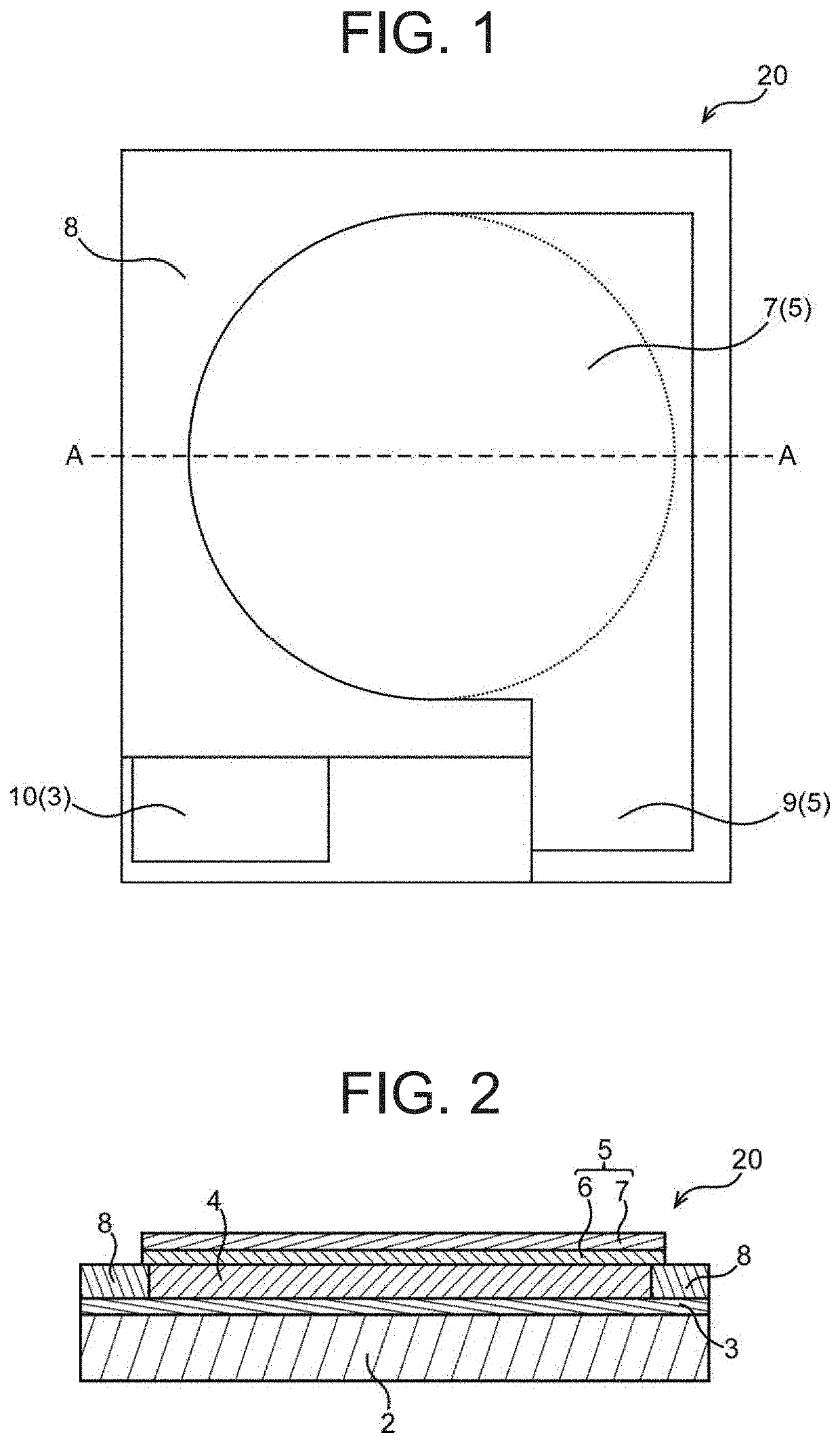
[0031]FIG. 1 is a schematic top view of an electron emission element of this embodiment, and FIG. 2 is a schematic sectional view of the electron emission element taken along a broken line A-A of FIG. 1.

[0032]The electron emission element 20 of this embodiment includes a lower electrode 3, a surface electrode 5, and a silicone resin layer 4 disposed between the lower electrode 3 and the surface electrode 5, the surface electrode 5 includes a silver layer 6, and the silver layer 6 is in contact with the silicone resin layer 4.

[0033]The electron emission element 20 of this embodiment can have an insulating layer 8 having an opening that defines an electron emission region of the electron emission element 20.

[0034]The electron emission element 20 is an element that emits electrons from the electron emission region of the surface electrode 5 into air, gas, a reduced pressure atmosphere, and the like. The electrons emitted from the electron emission region charge gas to generate anions i...

second embodiment

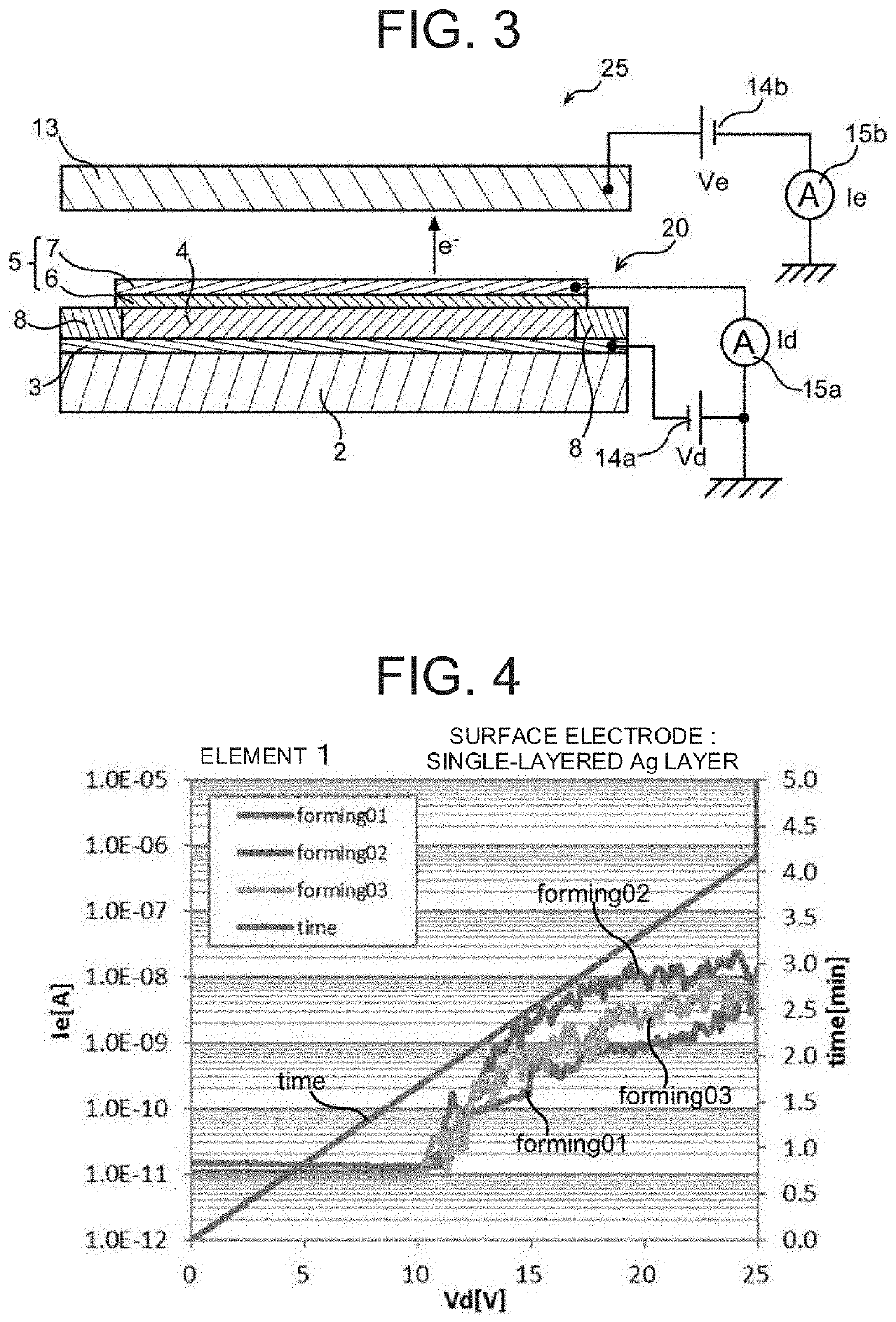
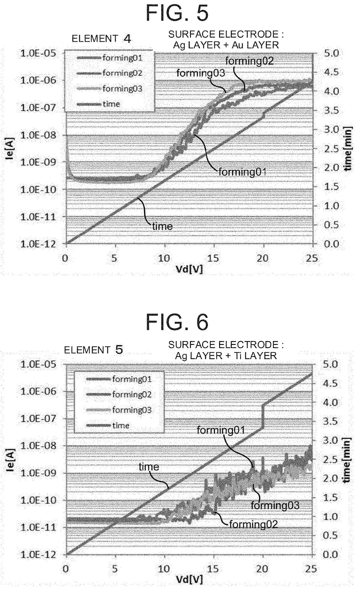
[0055]FIG. 3 is a schematic sectional view of an electron emission device of this embodiment. FIG. 3 also illustrates a circuit diagram illustrating an electrical configuration of the electron emission device.

[0056]The electron emission device 25 of this embodiment includes an electron emission element 20, an electric field generating electrode 13, and power supplies 14a and 14b. The power supply 14a is provided so as to apply a voltage between a lower electrode 3 and a surface electrode 5. The power supply 14b is provided so as to apply a voltage between the electron emission element 20 and the electric field generating electrode 13.

[0057]Further, the electron emission device 25 can include an ammeter 15a provided to so as to measure a current that flows between the lower electrode 3 and the surface electrode 5, or an ammeter 15b provided so as to measure a current caused to flow by electrons that are emitted from the electron emission element 20 and that reach the electric field g...


PUM

PropertyMeasurementUnit
thicknessaaaaaaaaaa
thicknessaaaaaaaaaa
thicknessaaaaaaaaaa

Abstract

An electron emission element of the present invention includes a lower electrode, a surface electrode, and a silicone resin layer disposed between the lower electrode and the surface electrode, wherein the surface electrode includes a silver layer, and the silver layer is in contact with the silicone resin layer.

Description

BACKGROUND OF THE INVENTIONField of the Invention[0001]The present invention relates to an electron emission element and a method for manufacturing the same.Description of the Background Art[0002]An electron emission element provided with an intermediate layer between an electrode substrate and a surface electrode is known (see, for example, Japanese Unexamined Patent Application Publication No. 2016-136485). A silicone resin layer containing silver nanoparticles is used as the intermediate layer.[0003]In this electron emission element, a current is allowed to pass through the intermediate layer by an electric field generated by application of a voltage between the two electrodes. At this time, some of electrons pass through the surface electrodes, and are emitted into the atmosphere. Such an electron emission element can be used as a charging device for charging a photoconductor, a light emitting device, or the like.[0004]However, in a conventional electron emission element, silver...

Claims


Application Information

Patent Timeline
Patent Type & Authority Patents(United States)
IPC IPC(8): H01J1/30H01J9/02
CPCH01J1/30H01J9/022H01J2209/012
Inventor SHINKAWA, KOHJIIWAMATSU, TADASHITSUJINO, KAZUYAABEYSINGHE, RESHAN MADUKAKOSAKA, TOMOHIRO
Owner SHARP KK
Why Eureka
Try Eureka