Film-shaped firing material and film-shaped firing material with support sheet

a technology of film-shaped firing materials and supporting sheets, which is applied in the direction of film/foil adhesives without carriers, film/foil adhesives, synthetic resin layered products, etc., can solve the problems of heat generation from semiconductor elements and affect heat dissipation efficiency, etc., to suppress chipping and contamination of wafers during dicing, and excellent thickness stability

Active Publication Date: 2022-03-08
LINTEC CORP
View PDF10 Cites 0 Cited by
  • Summary
  • Abstract
  • Description
  • Claims
  • Application Information

AI Technical Summary

Benefits of technology

[0029]According to the present invention, it is possible to provide a film-shaped firing material which has excellent thickness stability and is capable of suppressing chipping and contamination of a wafer during dicing. Further, it is possible to provide a film-shaped firing material with a support sheet which includes the film-shaped firing material, and is used for sinter bonding of chips of a semiconductor element or the like, a film-shaped firing material with a support sheet which is capable of suppressing chipping and contamination of a wafer during dicing, and is capable of stably picking up diced chips with the film-shaped firing material; and a method of manufacturing a semiconductor device obtained by using the film-shaped firing material with a support sheet.

Problems solved by technology

Since a power semiconductor element is used in a high-voltage and high-current environment, generation of heat from the semiconductor element may become a problem.
However, in a case where the thermal conductivity in a portion where the heat sink and the semiconductor element are bonded is not excellent, efficient heat dissipation is affected.

Method used


Image

  • Film-shaped firing material and film-shaped firing material with support sheet
  • Film-shaped firing material and film-shaped firing material with support sheet
  • Film-shaped firing material and film-shaped firing material with support sheet

Examples


first embodiment

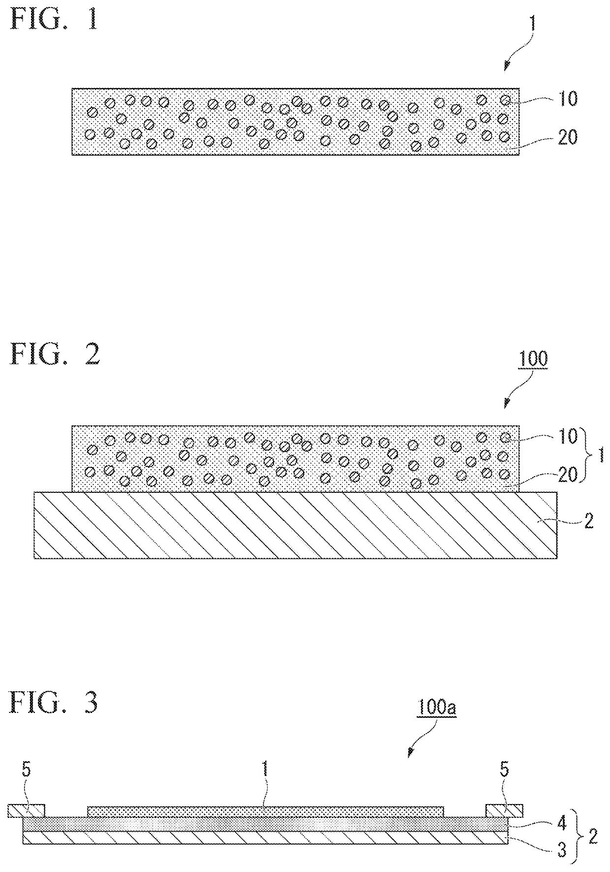
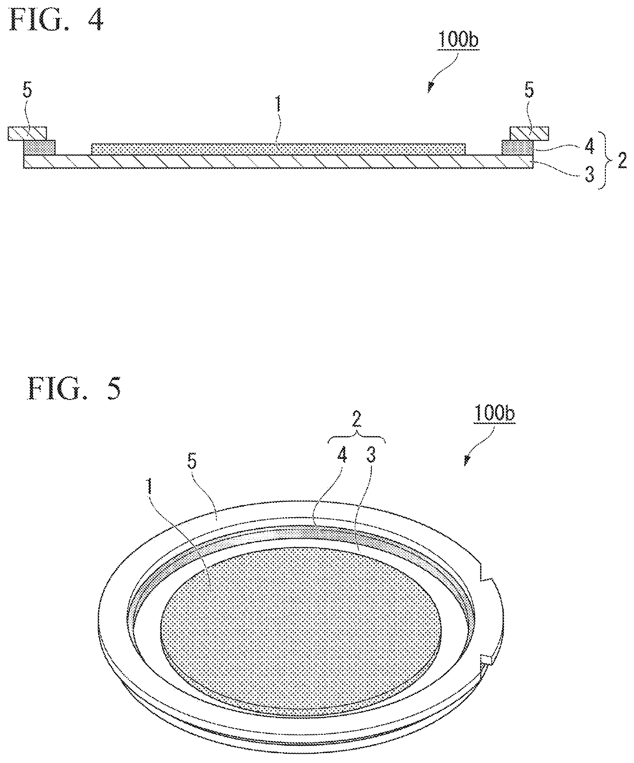
[0131]A film-shaped firing material with a support sheet according to the present embodiment includes the above-described film-shaped firing material and a support sheet provided on at least one side (surface) of the film-shaped firing material. The support sheet is formed such that a pressure-sensitive adhesive layer is provided on the entire surface or the outer peripheral portion of a base film, and it is preferable that the film-shaped firing material be provided on the pressure-sensitive adhesive layer. The film-shaped firing material may be provided by being brought into direct contact with the pressure-sensitive adhesive layer or provided by being brought into direct contact with the base film. By employing the present form, the material can be used as a dicing sheet used at the time of dividing a semiconductor wafer into chips. Further, the film-shaped firing material having the same shape as the shape of chip can be processed by being divided together with the semiconductor...

second embodiment

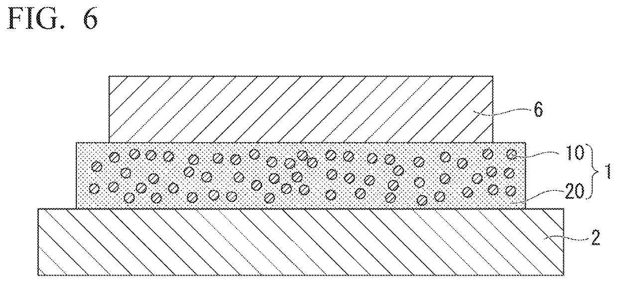
[0157]A film-shaped firing material with a support sheet of the present embodiment includes a film-shaped firing material and a support sheet which is provided on at least one side (surface) of the film-shaped firing material, in which an adhesive force (a2) of the film-shaped firing material to the support sheet is smaller than an adhesive force (a1) of the film-shaped firing material to a semiconductor wafer, the adhesive force (a1) is 0.1 N / 25 mm or greater, and the adhesive force (a2) is in a range of 0.1 N / 25 mm to 0.5 N / 25 mm. For example, in a laminate formed by laminating the film-shaped firing material with a support sheet according to the present embodiment and the semiconductor wafer illustrated in FIG. 6, the adhesive force (a2) of the film-shaped firing material to the support sheet is smaller than the adhesive force (a1) of the film-shaped firing material to the semiconductor wafer, the adhesive force (a1) is 0.1 N / 25 mm or greater, and the adhesive force (a2) is in a ...

examples

[0239]Hereinafter, the present invention will be described in detail based on the examples, and the scope of the present invention is not limited to these examples and the like.


PUM

PropertyMeasurementUnit
breaking elongationaaaaaaaaaa
glass transition temperatureaaaaaaaaaa

Abstract

The present invention provides a film-shaped firing material 1 including sinterable metal particles 10, and a binder component 20, in which a content of the sinterable metal particles 10 is in a range of 15% to 98% by mass, a content of the binder component 20 is in a range of 2% to 50% by mass, a tensile elasticity of the film-shaped firing material at 60° C. is in a range of 4.0 to 10.0 MPa, and a breaking elongation thereof at 60° C. is 500% or greater; and a film-shaped firing material with a support sheet including the film-shaped firing material 1 which contains sinterable metal particles and a binder component, and a support sheet 2 which is provided on at least one side of the film-shaped firing material, in which an adhesive force (a2) of the film-shaped firing material to the support sheet is smaller than an adhesive force (a1) of the film-shaped firing material to a semiconductor wafer, the adhesive force (a1) is 0.1 N / 25 mm or greater, and the adhesive force (a2) is in a range of 0.1 N / 25 mm to 0.5 N / 25 mm.

Description

TECHNICAL FIELD[0001]The present invention relates to a film-shaped firing material and a film-shaped firing material with a support sheet.[0002]This application is the U.S. national phase of International Application No. PCT / JP2018 / 032763 filed on Sep. 4, 2018 which designated the U.S. and claims priority to Japanese Patent Application No. 2017-177653, filed on Sep. 15, 2017, Japanese Patent Application No. 2018-94575, filed on May 16, 2018, and Japanese Patent Application No. 2018-98014, filed on May 22, 2018, the entire contents of each of which are incorporated herein by reference.BACKGROUND ART[0003]In recent years, with the high voltage and high current of automobiles, air conditioners, and personal computers, the demand for power semiconductor elements (power devices) to be mounted on these has increased. Since a power semiconductor element is used in a high-voltage and high-current environment, generation of heat from the semiconductor element may become a problem.[0004]In t...

Claims


Application Information

Patent Timeline
Patent Type & Authority Patents(United States)
IPC IPC(8): C09J7/10C09J11/04H01L21/683H01L21/78H01L23/00
CPCC09J7/10C09J11/04H01L21/6835H01L21/78H01L24/27H01L24/29H01L24/83C09J2203/326C09J2400/16C09J2433/00H01L2221/68327H01L2221/68386H01L2224/27002H01L2224/27003H01L2224/8384H01L2224/83191H01L2924/20102H01L2924/20103B32B27/00B32B27/18C09J7/00C09J201/00H01L21/52H01L2224/29298B22F7/04B22F2998/10B32B33/00H01B1/22H01L21/6836H01L24/32H01L24/92H01L24/94H01L2221/68336H01L2224/271H01L2224/27436H01L2224/2908H01L2224/29082H01L2224/29083H01L2224/29084H01L2224/2929H01L2224/29324H01L2224/29338H01L2224/29339H01L2224/29344H01L2224/29355H01L2224/2936H01L2224/29364H01L2224/29366H01L2224/29369H01L2224/29386H01L2224/29387H01L2224/2939H01L2224/32245H01L2224/83192H01L2224/83203H01L2224/83907H01L2224/92H01L2224/94H01L2224/27H01L2924/00014H01L2924/0541H01L2924/01047H01L2924/0635H01L2924/00012H01L2224/83H01L2924/013H01L2924/05432H01L2924/05381H01L2924/05442H01L2924/054H01L2924/01028H01L2924/01046H01L2924/01078H01L2924/05341H01L2924/01079H01L2924/068H01L2924/01014H01L2924/0549H01L2924/0532H01L2924/01056B22F1/10B22F3/22B22F3/10B22F7/08B82Y30/00
Inventor ICHIKAWA, ISAONAKAYAMA, HIDEKAZUSATO, AKINORI
Owner LINTEC CORP
Why Eureka
Try Eureka