
Chip package and power module

a power module and chip technology, applied in the direction of printed circuit grounding, semiconductor/solid-state device details, cross-talk/noise/interference reduction, etc., can solve the disadvantage of miniaturization of placing the grounding pad on the top surface of the chip package, the conductive wires are prone to interfering, etc., to reduce the material cost and manufacturing cost of the conductive wires, and reduce the resistance value and noise

Active Publication Date: 2022-04-19
XINTEC INC
View PDF21 Cites 0 Cited by
  • Summary
  • Abstract
  • Description
  • Claims
  • Application Information

AI Technical Summary

Benefits of technology

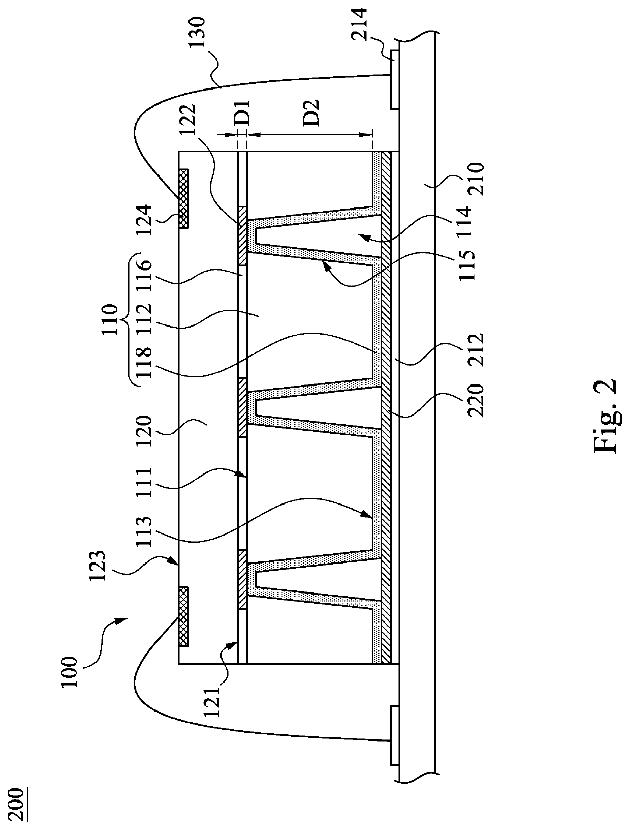
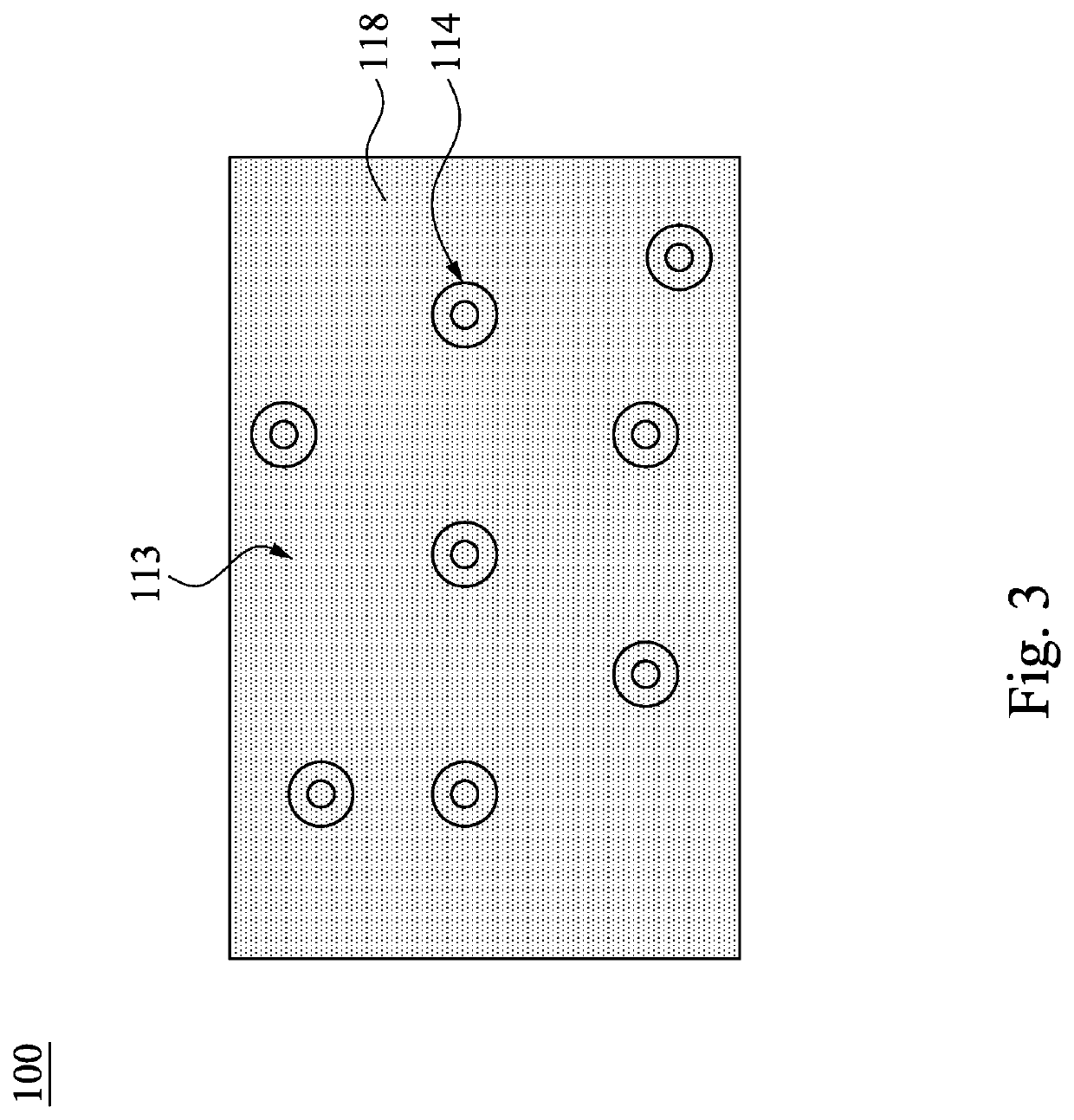
The present invention provides a chip package design that allows for better grounding, reduced resistance and noise, and smaller size. The chip package has a high voltage withstanding substrate with a grounding layer that covers the bottom surface and sidewall of the substrate. The grounding layer in the through hole is connected to the device chip's grounding pad, which in turn is connected to the printed circuit board's grounding region. This eliminates the need for wire bonding and reduces material and manufacturing costs. The chip package can also have conductive pads and wires without interference from the grounding pad and layer. Overall, this invention allows for better grounding, reduced resistance and noise, and smaller size of chip packages.

Problems solved by technology

As a result, not only the interference between the conductive wires is prone to occur, but also the material cost and manufacturing cost of the conductive wires cannot be reduced.
In addition, due to the limited area of the chip package, placing the grounding pad on the top surface of the chip package is disadvantageous for miniaturization.

Method used


Image

  • Chip package and power module
  • Chip package and power module
  • Chip package and power module

Examples


Embodiment Construction

[0032]Reference will now be made in detail to the present embodiments of the invention, examples of which are illustrated in the accompanying drawings. Wherever possible, the same reference numbers are used in the drawings and the description to refer to the same or like parts.

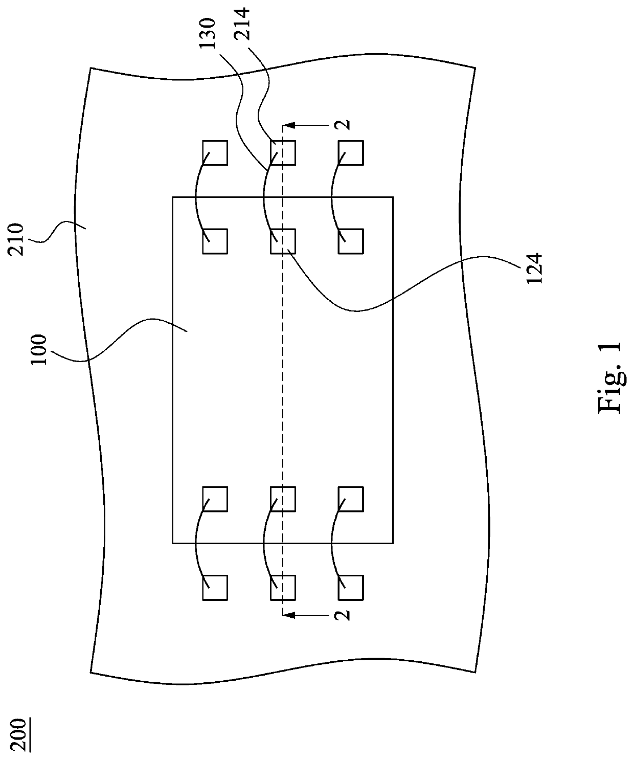
[0033]FIG. 1 is a top view of a power module 200 according to one embodiment of the present invention. FIG. 2 is a cross-sectional view of the power module 200 taken along line 2-2 shown in FIG. 1. As shown in FIG. 1 and FIG. 2, the power module 200 includes a printed circuit board 210 and a chip package 100. The printed circuit board 210 has a grounding region 212, and the grounding region 212 may be a conductive pad for grounding. The chip package 100 is located on the grounding region 212 of the printed circuit board 210. The grounding region 212 of the printed circuit board 210 may be a single large-area conductive structure or a plurality of small-area conductive structures, and the present invention is n...


PUM

PropertyMeasurementUnit
thicknessaaaaaaaaaa
thickness D2aaaaaaaaaa

Abstract

A chip package includes a high voltage withstanding substrate and a device chip. The high voltage withstanding substrate has a main body, a functional layer, and a grounding layer. The main body has a top surface, a bottom surface opposite the top surface, a through hole through the top surface and the bottom surface, and a sidewall surrounding the through hole. The functional layer is located on the top surface. The grounding layer covers the bottom surface and the sidewall. The device chip is located on the functional layer, and has a grounding pad that faces the main body. The grounding pad is electrically connected to the grounding layer in the through hole.

Description

RELATED APPLICATIONS[0001]This application claims priority to U.S. provisional Application Ser. No. 62 / 752,916, filed Oct. 30, 2018, which is herein incorporated by reference.BACKGROUNDField of Invention[0002]The present invention relates to a chip package and a power module having the chip package.Description of Related Art[0003]Generally speaking, a top surface of a chip package has a plurality of conductive pads. After the chip package is bonded to a printed circuit board, the conductive pad can be electrically connected to the printed circuit board by a wire bonding process. A portion of these conductive pads are associated with the grounding function of the chip package, and another portion is associated with the function of the chip package itself (e.g., power processing, fingerprint recognition, and image processing, etc.).[0004]However, in order to reduce a resistance value, each grounding pad of the chip package is usually bonded to more than two conductive wires to electri...

Claims


Application Information

Patent Timeline
Patent Type & Authority Patents(United States)
IPC IPC(8): H05K1/02H05K1/03H01L23/00
CPCH05K1/0215H01L24/29H05K1/0346H01L2224/29139H01L23/5286H01L23/5226H01L23/13H01L23/66H01L2224/04042H01L2224/04026H01L2224/48091H01L2224/48227H01L2924/3025H01L2224/73265H01L23/552H01L2224/06181H01L24/73H01L24/48H05K1/0254H05K1/181H05K2203/049H01L2224/08235H01L2224/73251H01L23/481H01L24/08H01L23/49872H01L23/49827H01L23/49833H01L2924/00014H01L2224/08H01L2224/48
Inventor LIU, TSANG-YULEE, PO-HANCHIEN, WEI-MING
Owner XINTEC INC
Learn More