Heat flow switching element

a switching element and heat flow technology, applied in the direction of electrical equipment, semiconductor devices, semiconductor/solid-state device details, etc., can solve the problems of large influence of convective heat transfer between materials, difficult design a size, and inability to avoid plastic deformation, etc., to achieve large change in thermal conductivity and high thermal responsiveness

Active Publication Date: 2022-06-14
MITSUBISHI MATERIALS CORP +1
View PDF19 Cites 0 Cited by
  • Summary
  • Abstract
  • Description
  • Claims
  • Application Information

AI Technical Summary

Benefits of technology

[0014]The present invention has been made in view of the above-described problems, and an object thereof is to provide a heat flow switching element which has a larger change in a thermal conductivity and has excellent thermal responsiveness.
[0031]That is, according to the heat flow switching element of the present invention, since the heat flow switching element includes an N-type semiconductor layer, an insulator layer laminated on the N-type semiconductor layer, and a P-type semiconductor layer laminated on the insulator layer, the amount of electric charges generated by application of an external voltage is large, and a large change in thermal conductivity and high thermal responsiveness can be obtained.

Problems solved by technology

The following problems remain in the above-described conventional technology.
That is, in the techniques described in Patent Documents 1 and 2, since the physical thermal contact due to the thermal expansion is used, reproducibility cannot be obtained, in particular, it is difficult to design a size due to a minute change, and it is not possible to avoid plastic deformation due to a mechanical contact pressure.
Also, there is a problem that an influence of convective heat transfer between materials is too large.
Further, in the technique described in Patent Document 3, there is a problem that an oxidation-reduction reaction which is a chemical reaction is used and thermal conduction is not stable due to poor thermal responsiveness.

Method used


Image

  • Heat flow switching element
  • Heat flow switching element
  • Heat flow switching element

Examples


example 1

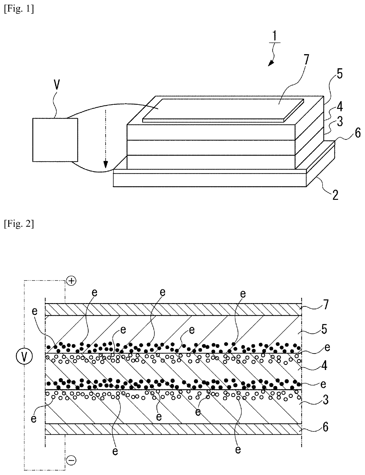
[0094]An insulator layer, a P-type semiconductor layer, and a P-side electrode were laminated on an N-type semiconductor layer using the following materials to form Example 1 of the present invention, and a change in the thermal conductivity was measured.

[0095]N-type semiconductor layer: Si substrate of N-type semiconductor (thickness of 0.5 mm)

[0096]Insulator layer: SiO2 (thickness of 100 nm)

[0097]P-type semiconductor layer: Si0.375Ge0.575Au0.05 (thickness of 40 nm)

[0098]P-side electrode: Mo (thickness of 100 nm)

[0099]It has been confirmed that each of SiO2 (thickness of 100 nm) and Si0.375Ge0.575Au0.05 (thickness of 40 nm) has a thermal conductivity of less than 2 W / mK in a single film.

[0100]Further, SiO2 (thickness of 100 nm) was formed by an RF sputtering method, and Si0.375Ge0.575Au0.05 (thickness of 40 nm) was formed by an MBE method.

[0101]An Au wire was connected to the Si substrate of the N-type semiconductor and Mo of the P-side electrode, and a voltage was applied. Further...

example 2

[0104]An N-type semiconductor layer, an insulator layer, a P-type semiconductor layer, and a P-side electrode were laminated on a substrate using the following materials to form Example 2 of the present invention, and a change in the thermal conductivity was measured.

[0105]Substrate: glass substrate (thickness of 0.5 mm)

[0106]N-type semiconductor layer: Si0.36Ge0.56P0.08 (thickness of 40 nm)

[0107]Insulator layer: SiO2 (thickness of 30 nm)

[0108]P-type semiconductor layer: Si0.375Ge0.575Au0.05 (thickness of 20 nm)

[0109]P-side electrode: Mo (thickness of 100 nm)

[0110]It has been confirmed that each of Si0.36Ge0.56P0.08 (thickness of 40 nm), SiO2 (thickness of 30 nm) and Si0.375Ge0.575Au0.05 (thickness of 20 nm) has a thermal conductivity of less than 2 W / mK in a single film.

[0111]Further, SiO2 (thickness of 30 nm) was formed by an RF sputtering method, and Si0.36Ge0.56P0.08 (thickness of 40 nm) and Si0.375Ge0.575Au0.05 (thickness of 20 nm) were formed by an MBE method.

[0112]An Au wire ...


PUM

PropertyMeasurementUnit
thicknessaaaaaaaaaa
thicknessaaaaaaaaaa
thicknessaaaaaaaaaa

Abstract

Provided is a heat flow switching element which has a larger change in a thermal conductivity and has excellent thermal responsiveness. The heat flow switching element includes an N-type semiconductor layer, an insulator layer laminated on the N-type semiconductor layer, a P-type semiconductor layer laminated on the insulator layer, an N-side electrode connected to the N-type semiconductor layer, and a P-side electrode connected to the P-type semiconductor layer. In particular, the insulator layer is formed of a dielectric. Also, a plurality of N-type semiconductor layers and P-type semiconductor layers are laminated alternately with the insulator layer interposed therebetween.

Description

CROSS REFERENCE TO RELATED APPLICATIONS[0001]This application is related to co-pending application: “HEAT FLOW SWITCHING ELEMENT” filed even date herewith in the names of Toshiaki FUJITA, Koya ARAI, Tsunehiro TAKEUCHI and Takuya MATSUNAGA, which claims priority to Japanese Application No. 2020-018679, filed Feb. 6, 2020; the above-identified application is assigned to the assignee of the present application and is incorporated by reference herein.BACKGROUND OF THE INVENTIONField of the Invention[0002]The present invention relates to a heat flow switching element which can actively control thermal conduction with a bias voltage.Description of Related Art[0003]Conventionally, as a thermal switch for changing a thermal conductivity, for example, Patent Document 1 discloses a thermal diode in which two thermal conductors having different thermal expansion coefficients are lightly brought into contact with each other to change a flow of heat depending on a direction of a temperature grad...

Claims


Application Information

Patent Timeline
Patent Type & Authority Patents(United States)
IPC IPC(8): H01L35/32H01L23/34H01L35/30H01L35/10H01L35/04H01L35/08
CPCH01L35/32H01L23/34H01L35/04H01L35/08H01L35/10H01L35/30H10N10/82H10N10/81H10N10/17H10N10/13H10N10/851H10N10/817
Inventor FUJITA, TOSHIAKIARAI, KOYATAKEUCHI, TSUNEHIROMATSUNAGA, TAKUYA
Owner MITSUBISHI MATERIALS CORP
Why Eureka
Try Eureka