Electroconductive member, process cartridge, and image forming apparatus

a technology of image forming apparatus and process cartridge, which is applied in the direction of electrographic process, instruments, corona discharge, etc., can solve the problem of insufficient leveling of minute potential unevenness, and achieve the effect of high-quality electrophotographi

Active Publication Date: 2022-07-12
CANON KK
View PDF108 Cites 0 Cited by
  • Summary
  • Abstract
  • Description
  • Claims
  • Application Information

AI Technical Summary

Benefits of technology

[0010]In addition, another aspect of the present disclosure is directed to providing a process cartridge that contributes to the formation of a high-quality electrophotographic image. Still another aspect of the present disclosure is directed to providing an electrophotographic image forming apparatus capable of forming a high-quality electrophotographic image.

Problems solved by technology

Specifically, when the charging member according to Japanese Patent Application Laid-Open No. 2002-3651 is subjected to the formation of an electrophotographic image, it is not possible to sufficiently level the minute potential unevenness formed on the surface of the body to be charged up to the charging step, and an electrophotographic image (hereinafter, also referred to as “ghost image”) in which an image that is not supposed to be originally formed due to the potential unevenness is superimposed on the original image may be formed in some cases.

Method used


Image

  • Electroconductive member, process cartridge, and image forming apparatus
  • Electroconductive member, process cartridge, and image forming apparatus
  • Electroconductive member, process cartridge, and image forming apparatus

Examples


example 1

[0238](1. Manufacture of Unvulcanized Rubber Mixture for Forming Domain (CMB))

[0239][1-1. Preparation of Unvulcanized Rubber Mixture]

[0240]The materials indicated in Table 1 were mixed in the blending amounts indicated in Table 1 using a 6-liter pressure kneader (product name: TD6-15MDX, available from Toshin) to obtain CMB. The mixing conditions were a filling rate of 70 vol %, a blade rotation speed of 30 rpm, and 20 minutes of time duration.

[0241]

TABLE 1Blendingamount(parts byRaw material namemass)Raw material Styrene butadiene rubber100rubber(Product name: TUFDENE 1000, available from Asahi Kasei Corporation)ElectronicCarbon black80electroconductive (Product name: TOKABLACK #5500, agentavailable from Tokai Carbon Co., Ltd.)Vulcanization Zinc oxide5acceleration aid(Product name: Zinc oxide, available fromSakai Chemical Industry Co., Ltd.)Processing aidZinc stearate2(Product name: SZ-2000, available from Sakai Chemical Industry Co., Ltd.)

[0242][1-2. Preparation of Rubber Mixture f...

example 2 to example 38

[0325]Electroconductive members A2 to A38 are manufactured in the same manner as in Example 1 except that the materials and conditions indicated in Tables 5A-1 to 5A-4 are used for the raw rubber, the electroconductive agent, the vulcanizing agent, and the vulcanization accelerator.

[0326]For details of the materials indicated in Tables 5A-1 to 5A-4, the rubber material is indicated in Table 5B-1, the electroconductive agent is indicated in Table 5B-2, and the vulcanizing agent and accelerator are indicated in Table 5B-3.

[0327]Further, in Example 36, using a compound available from Toho Tenax (product name: rPEEK CF30), it is possible to mold into a round bar type which can be molded in the same shape as the support in Example 1 at a mold temperature of 380° C. A round bar made of the obtained electroconductive resin (total length 252 mm, outer diameter 6 mm) was used as a support.

[0328]In Example 37, the following adhesive (metalloc (metalloc N-33, available from Toyo Kagaku Kenkyus...

example 39

[0341]An electroconductive roller B1 was manufactured in the same manner as in Example 1 except that the diameter of the electroconductive support was changed to 5 mm and the outer diameter of the electroconductive member after polishing was 10.0 mm.

[0342]The electroconductive roller B1 was used as a transfer member for the following evaluations.

[0343]As an electrophotographic apparatus, an electrophotographic laser printer (product name: Laserjet M608dn, available from HP) was prepared.

[0344]First, the electroconductive roller B1 and the laser printer were left in an environment of 23° C. and 50% for 48 hours for the purpose of adjusting to the measurement environment.

[0345]Next, the electroconductive roller B1 was incorporated into the laser printer as a transfer member. In order to evaluate in a high-speed process, the laser printer was modified so that the number of output sheets per unit time was 75 sheets / minute with A4 size paper, which was larger than the number of original ...
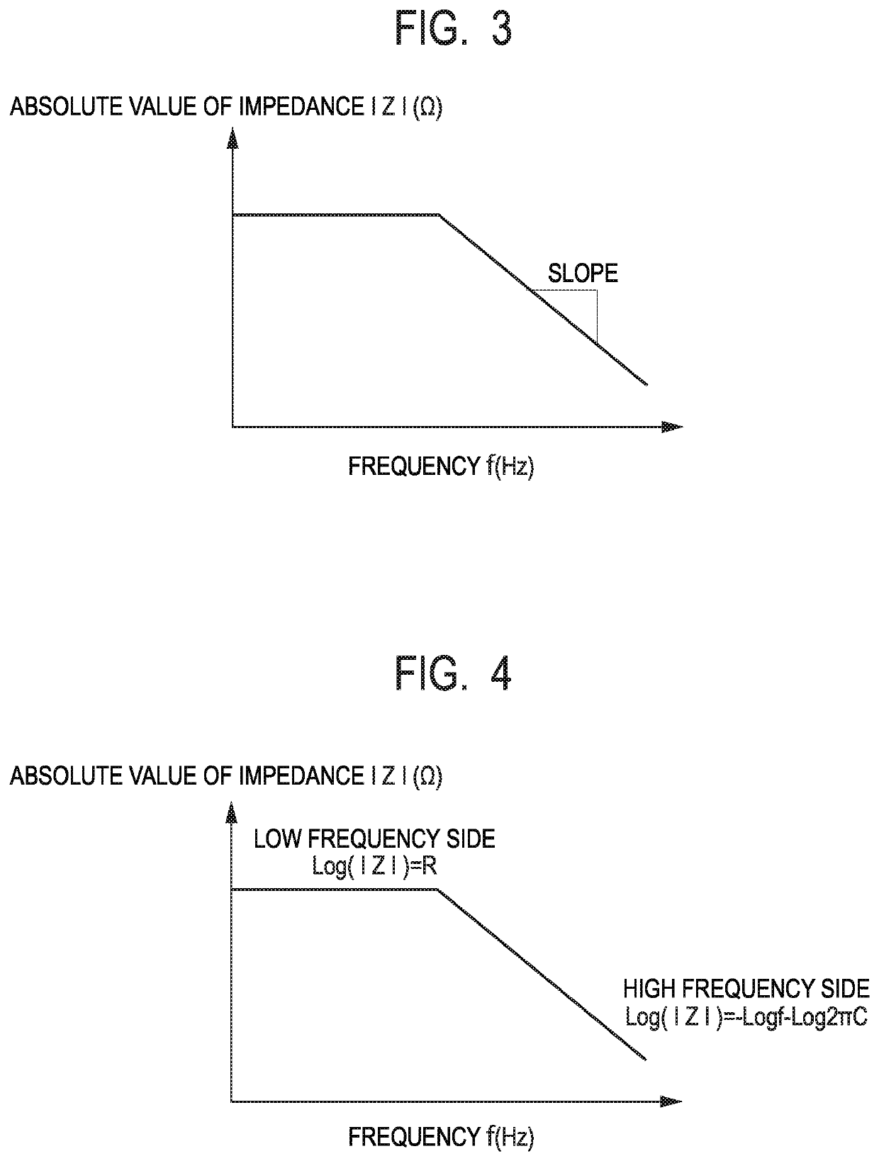

PUM

PropertyMeasurementUnit
impedanceaaaaaaaaaa
frequencyaaaaaaaaaa
frequencyaaaaaaaaaa

Abstract

Provided is an electrophotographic electroconductive member including an electroconductive support and an electroconductive layer on the support, an electroconductive member is used, in which an electroconductive layer has a matrix comprising a first rubber, and domains dispersed in the matrix, the domains each comprising a second rubber and an electronic electroconductive agent, and for impedance measured by applying an AC voltage with an amplitude of 1 V to the electroconductive layer while varying frequencies between 1.0×10⁻² Hz to 1.0×10⁷ Hz under a specific environment, when a double logarithmic plot with a frequency on an abscissa and an impedance on an ordinate is obtained, a slope on a high frequency side is −0.8 or more and −0.3 or less, and the impedance a low frequency side is from 1.0×10³ to 1.0×10⁷Ω.

Description

CROSS-REFERENCE TO RELATED APPLICATIONS[0001]This application is a Continuation of International Patent Application No. PCT / JP2019 / 016300, filed Apr. 16, 2019, which claims the benefit of Japanese Patent Application No. 2018-079952, filed Apr. 18, 2018, Japanese Patent Application No. 2019-032936, filed Feb. 26, 2019, and Japanese Patent Application No. 2019-069097, filed Mar. 29, 2019, all of which are hereby incorporated by reference herein in their entirety.BACKGROUND[0002]The present disclosure relates to an electrophotographic electroconductive member that can be used as a charging member, a developing member, or a transfer member in an electrophotographic image forming apparatus, a process cartridge, and the electrophotographic image forming apparatus.DESCRIPTION OF THE RELATED ART[0003]An electroconductive member such as a charging member, a transfer member, or a developing member has been used in an electrophotographic image forming apparatus. As the electroconductive member...

Claims


Application Information

Patent Timeline
Patent Type & Authority Patents(United States)
IPC IPC(8): G03G21/16G03G15/02C08K3/04C08K3/26C08L19/00G03G21/18
CPCG03G15/0233C08K3/04C08K3/26C08L19/00G03G21/1814C08K2003/265C08K2201/001C08L21/00C08L9/02G03G15/0818G03G15/1685
Inventor KIKUCHI, YUICHINISHIOKA, SATORUTAKASHIMA, KENJIYAMAUCHI, KAZUHIROKURACHI, MASAHIROFURUKAWA, TAKUMIWATANABE, HIROAKITERADA, KENYATOMOMIZU, YUYANAKAZAWA, TOSHIMITSU
Owner CANON KK
Why Eureka
Try Eureka