

Etching apparatus for manufacturing semiconductor devices
a technology for etching apparatus and semiconductor devices, which is applied in lighting and heating apparatus, charge manipulation, furnaces, etc., can solve the problems of high risk of contamination of the upward-facing processing surface of the wafer, failure of the etching process, and productivity drop
- Summary
- Abstract
- Description
- Claims
- Application Information
AI Technical Summary
Benefits of technology
Problems solved by technology
Method used
Image

Examples
Embodiment Construction
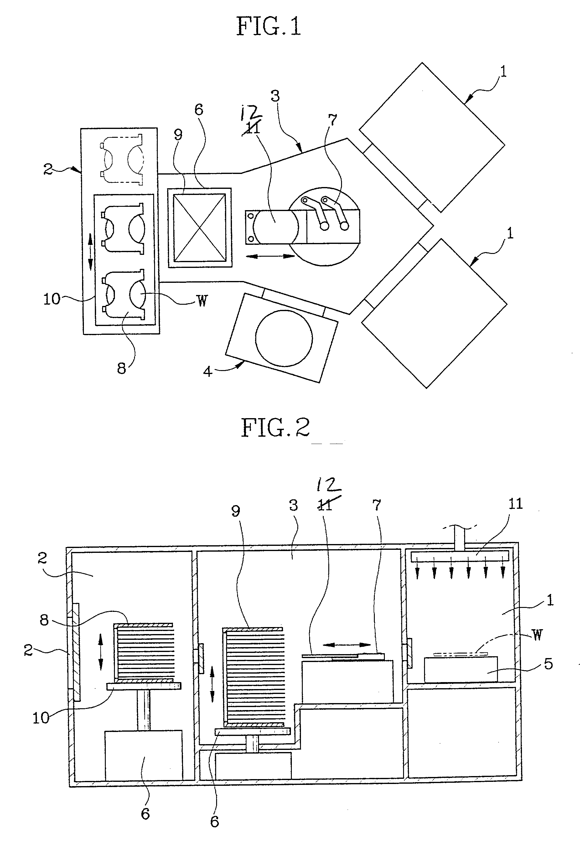
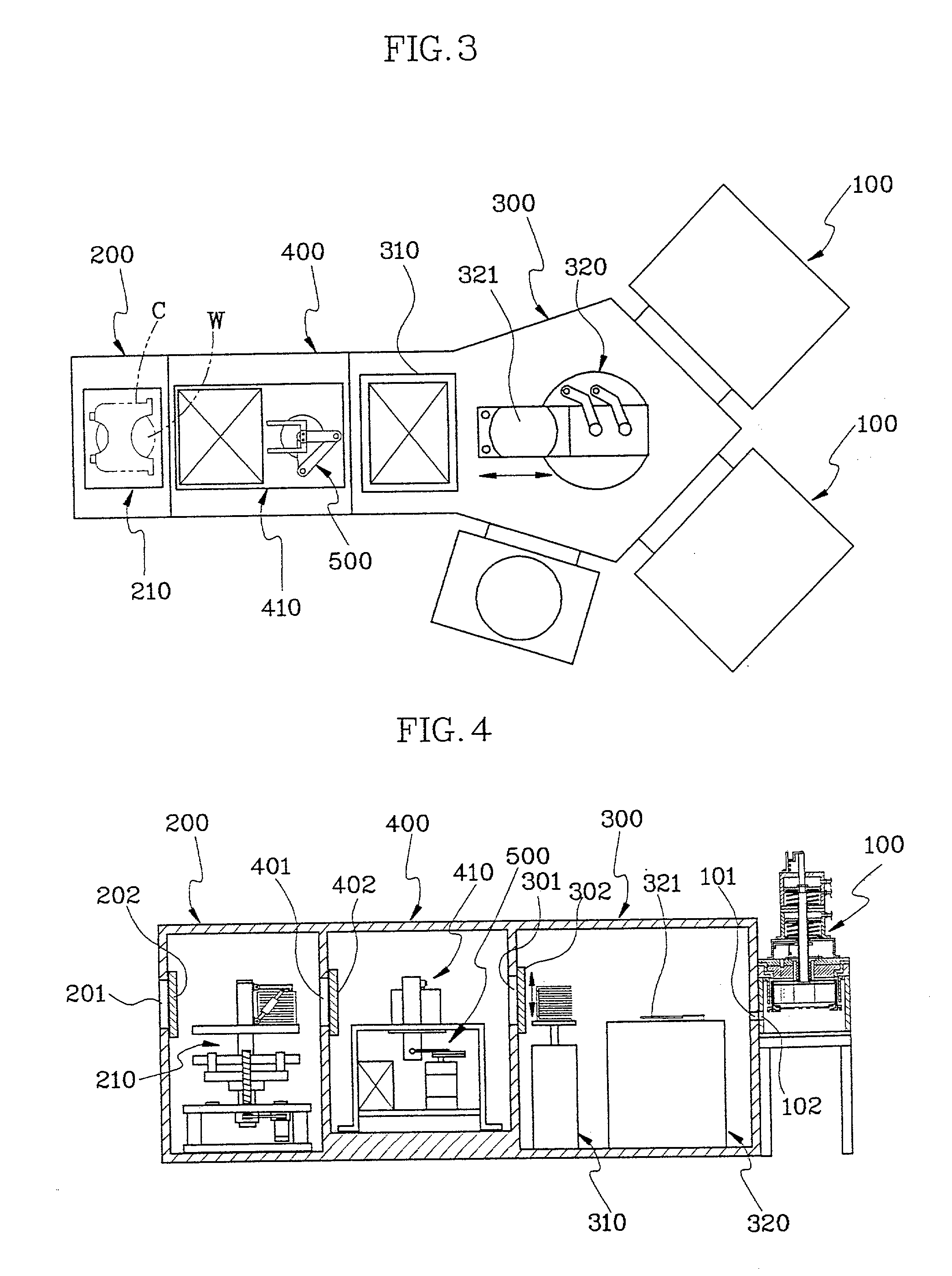
[0038] An etching apparatus for manufacturing semiconductor devices will be hereinafter described in detail with reference to FIG. 3 through FIG. 19.
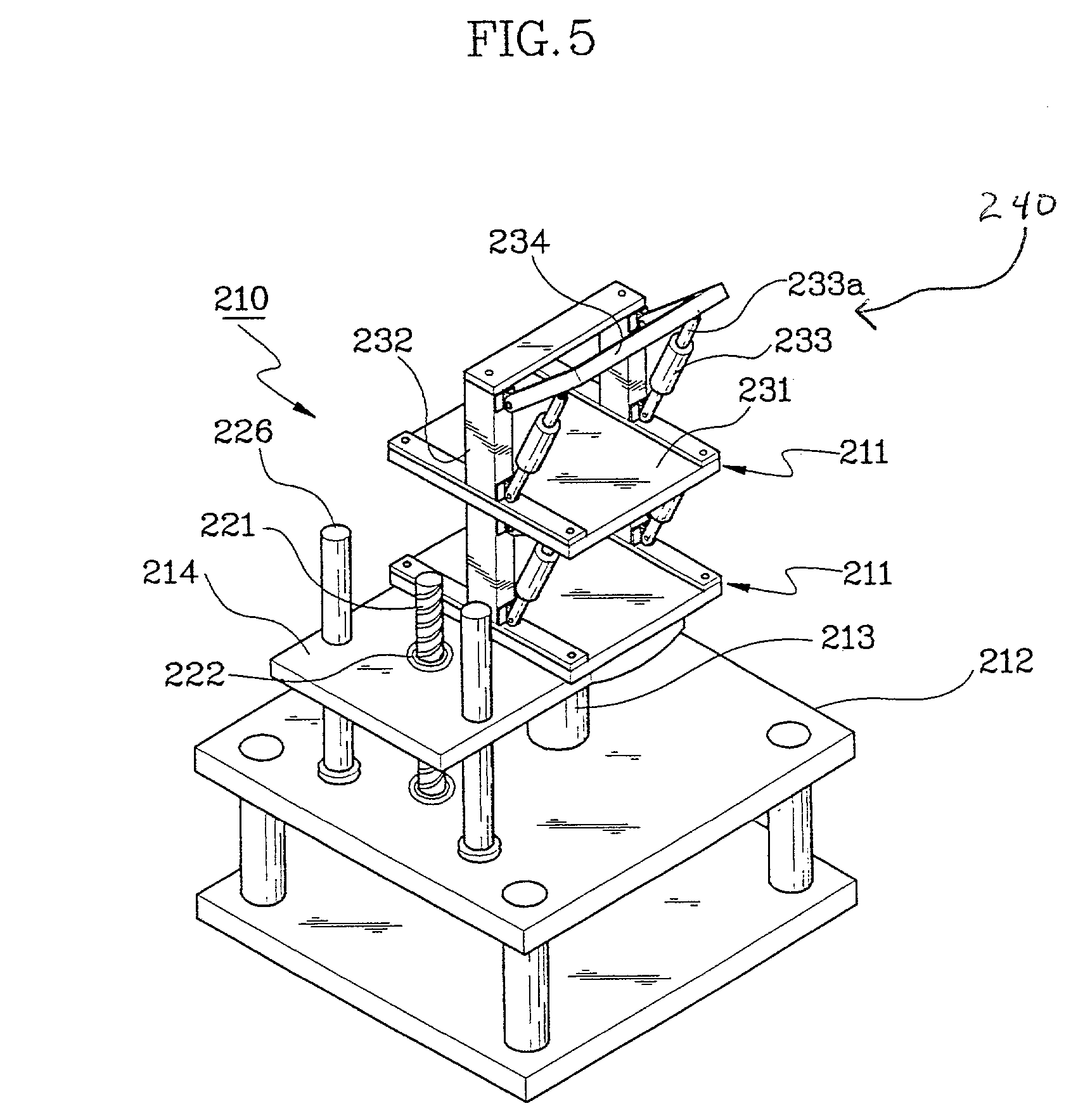
[0039] As illustrated in FIGS. 3 and 4, the etching apparatus of the invention includes: one or more process chambers 100 for performing the etching process, in which the surface of a wafer faces down. A cassette supplying chamber 200 supplies the wafer W to the process chamber 100. The cassette supplying chamber 200 has a cassette supply table 210 on which a cassette C is loaded with multiple wafers W stacked therein so that their processing surfaces face down. A load lock chamber 300, installed between the process chamber 100 and the wafer supply chamber 200, receives the wafer W stored in cassette C from the cassette supply chamber 200, which is maintained under atmospheric conditions, and transfers the wafer W to the process chamber 100, which is maintained under a high vacuum. Inside the load lock chamber 300 there is an elevator 3...
PUM
| Property | Measurement | Unit |
|---|---|---|
| volume | aaaaa | aaaaa |
| restoring forces | aaaaa | aaaaa |
| air pressure | aaaaa | aaaaa |
Abstract
Description
Claims
Application Information