

Device for converting a photosignal into a voltage in image sensors with remote integrators
- Summary
- Abstract
- Description
- Claims
- Application Information
AI Technical Summary
Benefits of technology
Problems solved by technology
Method used
Image

Examples
Embodiment Construction
[0029] The object of the invention is to find a remedy to the drawbacks of the image sensors with remote integrators, as described earlier. For this purpose, it provides a device for voltage conversion of a photosignal, which may be used in image sensors with remote integrators, and which exhibits reduced conversion noise.
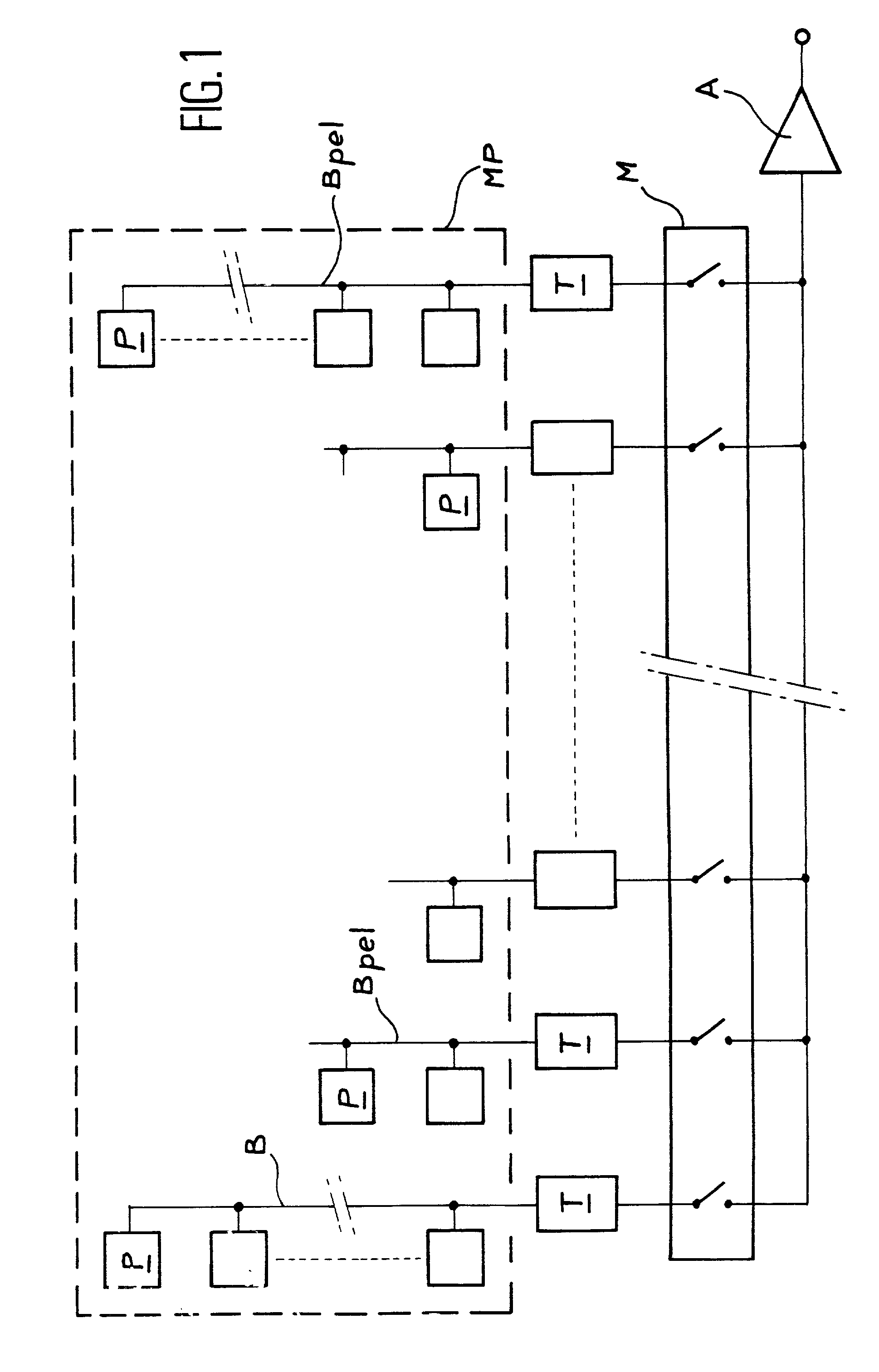
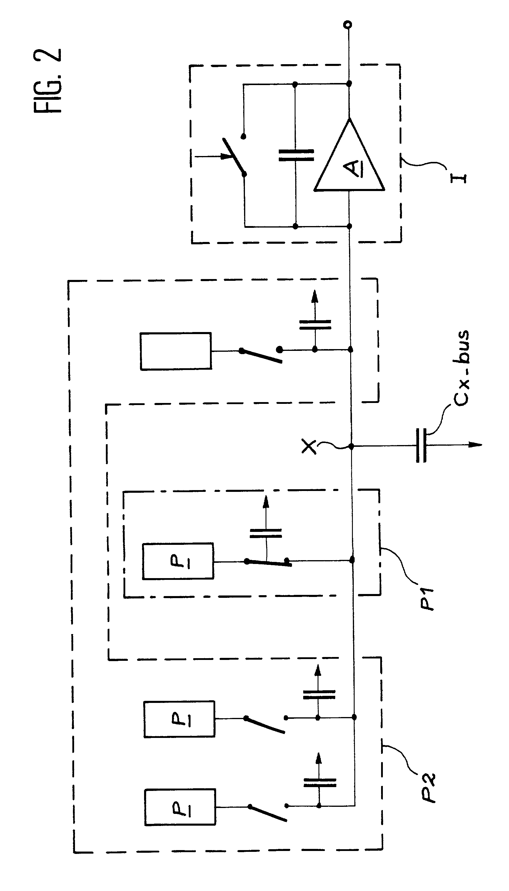
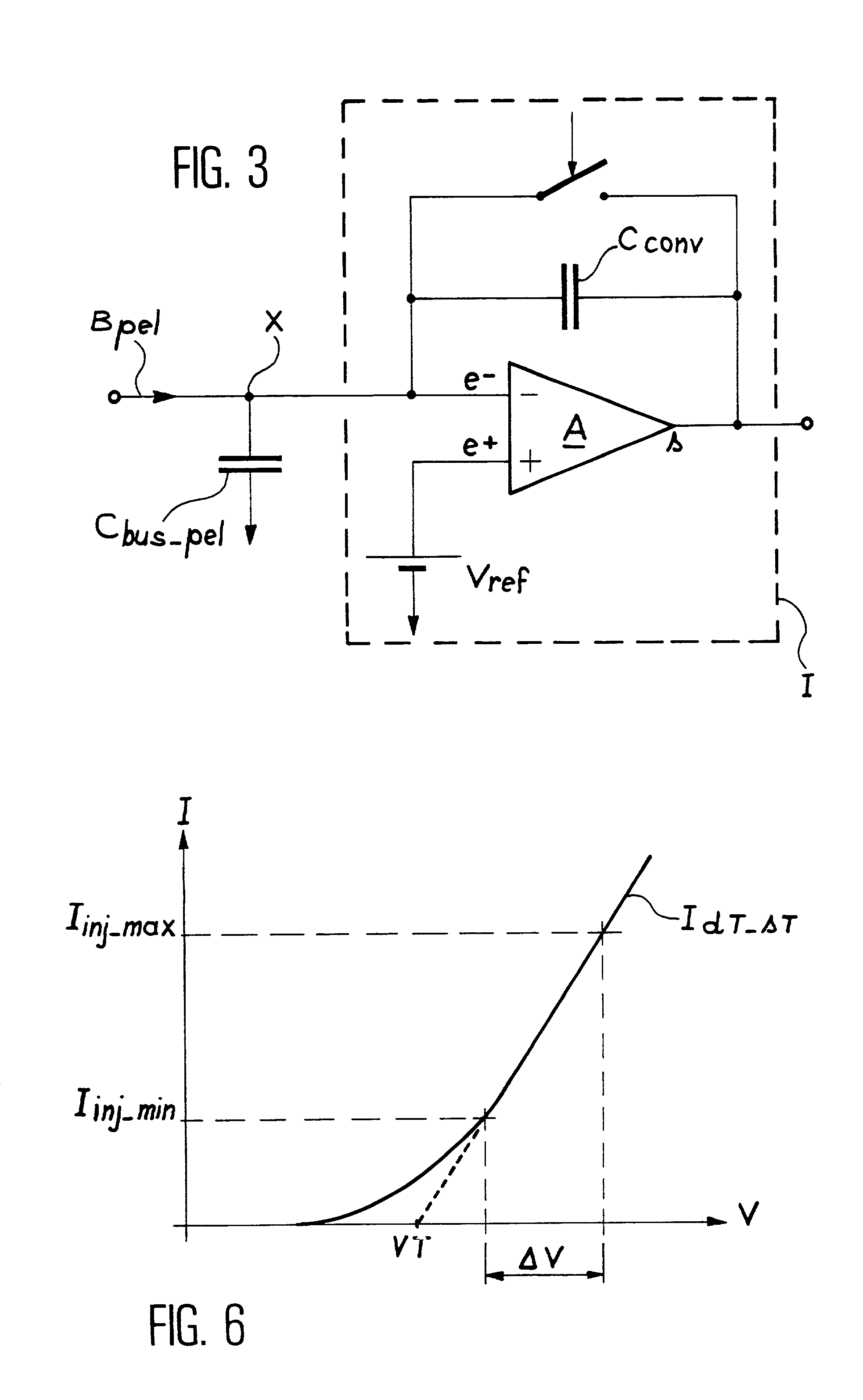
[0030] According to the invention, the conversion noise may be reduced if the effective fed-back capacitance at the input of the remote integrator is reduced significantly, without altering the voltage transfer function for the photosignal. This is achieved by inserting an impedance matching device with low output capacitance, between the end of the PEL bus (used for multiplexing the outputs of the elementary points of a same row) and the input of the integrator.
[0031] More specifically, the invention relates to an image sensor with matrix readout including a matrix of elementary photodetectors connected through at least a PEL bus to a remote integrator converting ...
PUM
 Abstract
Description
Claims
Application Information