Dual wafer load lock

a technology of load lock and wafer, which is applied in the direction of lighting and heating apparatus, charge manipulation, furniture, etc., can solve the problems of increasing the chance of particulate contamination and condensation on the substrate, long pump down time, and high cost of associated pumping hardwar

Inactive Publication Date: 2002-01-17
APPLIED MATERIALS INC
View PDF0 Cites 90 Cited by
  • Summary
  • Abstract
  • Description
  • Claims
  • Application Information

AI Technical Summary

Benefits of technology

0020] To facilitate understanding, identical reference numerals have been used, w

Problems solved by technology

However, due to the relatively large internal volume required to accommodate the entire substrate cassette, pump-down times are long and the associated pumping hardware is large and costly.
Additionally, venting of the large internal volume increase

Method used


Image

  • Dual wafer load lock
  • Dual wafer load lock
  • Dual wafer load lock

Examples


Embodiment Construction

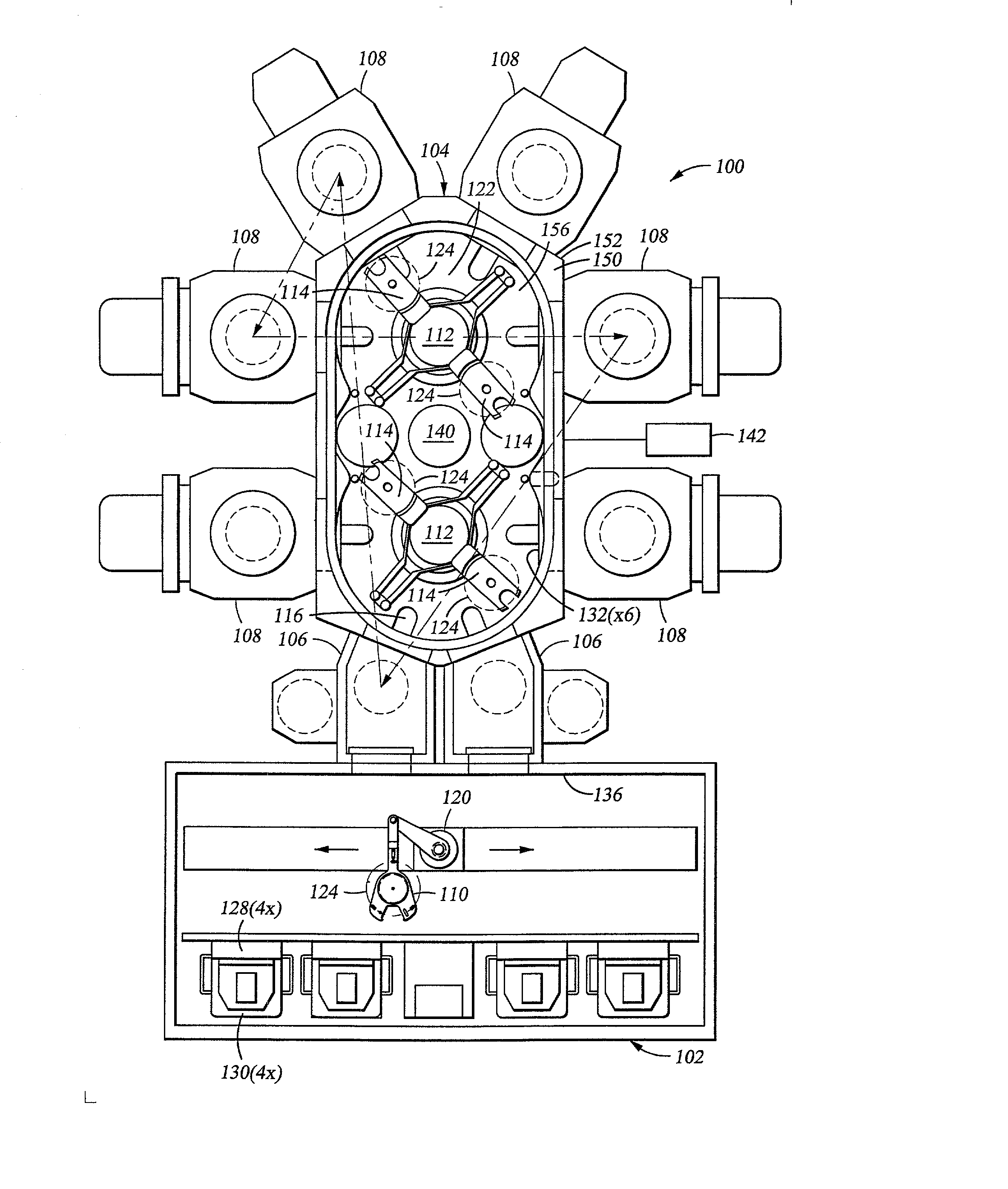
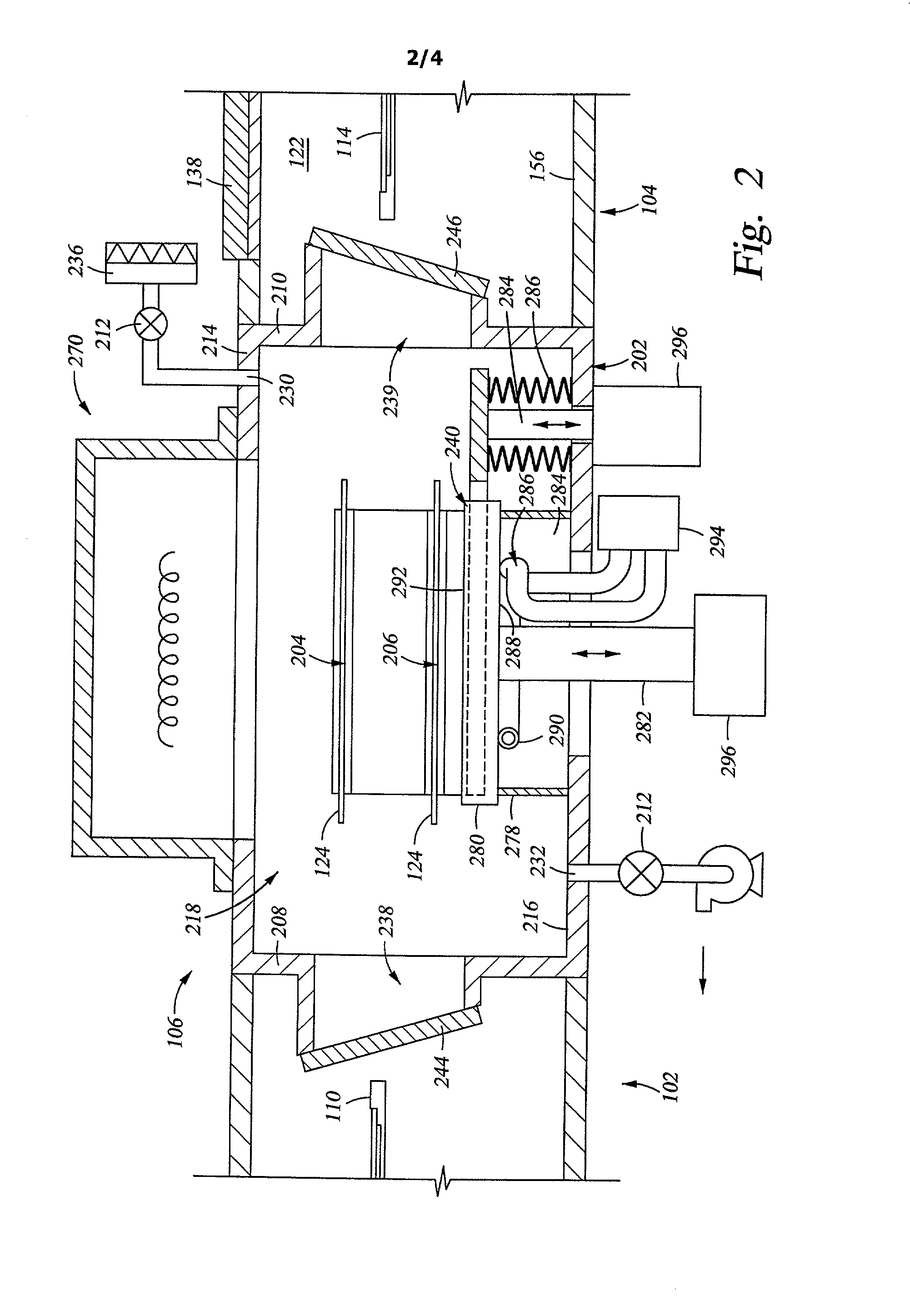
[0021] FIG. 1 depicts a processing system 100 that generally includes a factory interface 102, one or more load lock chambers 106, a plurality of process chambers 108 and a substrate transfer chamber 104. The transfer chamber 104 is generally used to transfer substrates 124 between a vacuum environment maintained in the transfer chamber 104 and a substantially ambient environment maintained in the factory interface 102. One example of a processing system that may be adapted to benefit from the invention is an ENDURA SL.RTM. processing platform, available from Applied Materials, Inc., of Santa Clara, Calif. Although the load lock chamber 106 is described in reference to the exemplary processing system 100 depicted in FIG. 1, the load lock chamber 106 has utility in other systems or wherever transfer of substrates between vacuum and ambient environments is desired.

[0022] The factory interface 102 generally includes an interface robot 120 and a plurality of bays 128. Each bay 128 is ad...


PUM

PropertyMeasurementUnit
Pressureaaaaaaaaaa
Volumeaaaaaaaaaa

Abstract

A method and apparatus for transferring a substrate between a first environment having a first pressure and a second environment having a vacuum pressure is provided. In one embodiment, the apparatus comprises a chamber body having a first port disposed in a first wall and a second port disposed in a second wall that seals the chamber from the first and second environments. A cooling plate, a first substrate holder and a second substrate holder are disposed within the chamber body. The cooling plate is disposed at the bottom of the chamber body. The first port and the second port are sequentially opened and the pressure within the load lock regulated to allow substrate to pass through the load lock. A window is disposed in the top of the chamber body that allows a metrology device to view the chamber volume.

Description

[0001] This application is a continuation-in-part of U.S. patent application Ser. No. 09 / 451,628, filed Nov. 30, 1999, which is hereby incorporated by reference in its entirety.BACKGROUND OF THE DISCLOSURE[0002] 1. Field of Invention[0003] The embodiments of the invention generally relate to a method and apparatus for transferring substrates in a semiconductor processing system.[0004] 2. Background of Invention[0005] Semiconductor substrate processing is typically performed by subjecting a substrate to a plurality of sequential processes to create devices, conductors and insulators on the substrate. These processes are generally performed in a process chamber configured to perform a single step of the production process. In order to efficiently complete the entire sequence of processing steps, a number of process chambers are typically coupled to a central transfer chamber that houses a robot to facilitate transfer of the substrate between the surrounding process chambers. A semicon...

Claims


Application Information

Patent Timeline
IPC IPC(8): B65G49/07H01L21/00C23C14/50H01L21/205H01L21/302H01L21/3065H01L21/677
CPCH01L21/67017H01L21/67109H01L21/67115H01L21/67161H01L21/67167Y10T29/413H01L21/6719H01L21/67196H01L21/67201H01L21/67253H01L21/67745H01L21/67184
Inventor KRAUS, JOSEPH ARTHURSTRASSNER, JAMES DAVID
Owner APPLIED MATERIALS INC
Why Eureka
Try Eureka