Method of manufacturing a contact plug in a semiconductor device

a technology of contact plugs and semiconductor devices, which is applied in the direction of semiconductor devices, electrical devices, transistors, etc., can solve the problems of increasing resistance, difficulty in applying polysilicon that has been used difficulty in using polysilicon as a contact plug, so as to improve the electrical characteristic of the device and prevent the effect of increasing resistan

Inactive Publication Date: 2002-01-24
INTELLECTUAL DISCOVERY CO LTD
View PDF0 Cites 9 Cited by
  • Summary
  • Abstract
  • Description
  • Claims
  • Application Information

AI Technical Summary

Benefits of technology

0007] The disclosed method is a method of manufacturing a contact plug in a semiconductor device capable of improving an electrical characteristic of the device, by which an impurity such as phosphorous (P) is thermally doped in-situ to increase t

Problems solved by technology

In a DRAM device of more than 1G bits, it is difficult to apply polysilicon that has been usually used as a contact plug since its contact area is miniatu

Method used


Image

  • Method of manufacturing a contact plug in a semiconductor device
  • Method of manufacturing a contact plug in a semiconductor device

Examples


Embodiment Construction

[0013] The disclosed method will be described in detail by way of a preferred embodiment with reference to accompanying drawings, in which like reference numerals are used to identify the same or similar parts.

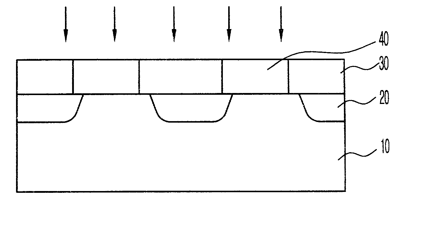
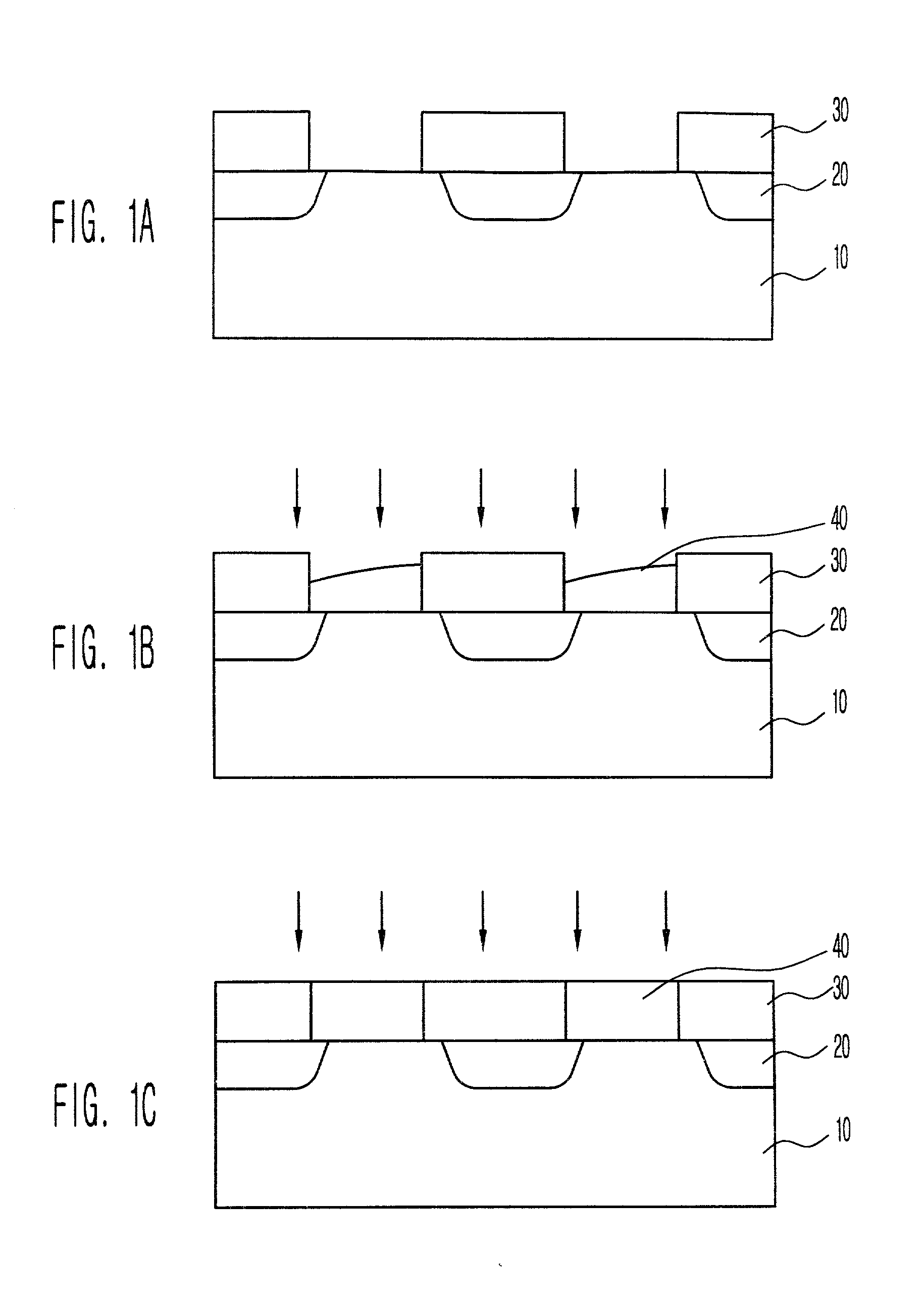
[0014] FIGS. 1A to 1C are cross-sectional views for explaining a method of manufacturing a contact plug in a semiconductor device according to the disclosed methodology.

[0015] Referring now to FIG. 1A, an interlayer insulating film 30 is formed on a semiconductor substrate 10 in which a device separation film 20 is formed. Then, the interlayer insulating film 30 is patterned to expose the junction surface of the semiconductor substrate 10, thus forming a contact hole.

[0016] Referring now to FIG. 1B, impurity is thermally doped into a SEG silicon layer for contact plug 40 while the SEG silicon layer for contact plug 40 is grown on the exposed surface of the semiconductor substrate 10. The thermal doping is performed when the SEG silicon layer for contact plug has been initially...


PUM


Abstract

A method of manufacturing a contact plug in a semiconductor device is disclosed. In-situ thermal doping of an impurity such as phosphorous (P) during the process by which polysilicon for a contact plug is formed by selective growth method and after in-situ doping after the growth process is employed in order to increase the concentration of the impurity in the contact plug. As a result, the disclosed method can reduce the interfacial resistance at the plug to improve the electrical characteristics of a device of more than 1G bits.

Description

[0001] 1. Field of the Invention[0002] The invention relates generally to a method of manufacturing a contact plug in a semiconductor device. More particularly, the present invention relates to a method of manufacturing a contact plug in a semiconductor device, which can reduce the resistance of a contact plug by preventing reduction in the impurity concentration of the contact plug formed by selective epitaxial growth (SEG) method.[0003] 2. Description of the Prior Art[0004] Using a plug select growth technology in a semiconductor device has been highly appreciated in view of reduction in cell size and simplification of process. In developing a DRAM device of more than 1G bits, however, in order to use the SEG process for forming a bit-line contact and a capacitor storage contact, the process condition are critical.[0005] In a DRAM device of more than 1G bits, it is difficult to apply polysilicon that has been usually used as a contact plug since its contact area is miniaturized. A...

Claims


Application Information

Patent Timeline
IPC IPC(8): H01L21/28H01L21/283H01L21/285H01L21/768H01L21/8242H01L27/108
CPCH01L21/28525H01L21/28562H01L21/283
Inventor SHIN, DONG SUKCHEONG, WOO SEOKKIM, BONG SOO
Owner INTELLECTUAL DISCOVERY CO LTD
Why Eureka
Try Eureka