

Multilayer thin film and its fabrication process as well as electron device
a multi-layer thin film and electron device technology, applied in the field of multi-layer thin films, can solve the problems of difficult to obtain satisfactory device performance, difficult to form a single-axis oriented ferroelectric thin film, and the properties of ferroelectric thin film formed on an si substrate are vastly inferior to those derived from ferroelectric's own properties
Inactive Publication Date: 2002-02-07
SNAPTRACK
View PDF0 Cites 35 Cited by
- Summary
- Abstract
- Description
- Claims
- Application Information
AI Technical Summary
Problems solved by technology
With polycrystal materials, it is difficult to obtain satisfactory device performance for the reason of physical quantity disturbances due to grain boundaries, and so epitaxial films as close to perfect single crystals as possible are now desired.
However, it is very difficult to form a uniaxially oriented ferroelectric thin film such as a (001) uniaxially oriented BaTiO.sub.3 film of good crystallographic properties on a semiconductor substrate such as an Si (100) substrate.
Usually, however, a ferroelectric thin film formed on an Si substrate as an example have properties vastly inferior to those derived from ferroelectric's own properties.
To apply a ferroelectric thin film to a device, therefore, any desired ferroelectric properties cannot be stably obtained without such stress reductions as mentioned above.
At such a thickness, the effect of elastic distortion due to the misfit vanishes into almost nothing; any satisfactory piezoelectric properties are no longer achieved.
However, this makes the fabrication process complicated, and offers some problems as well.
For instance, resonance characteristics become worse due to the presence of many layer interfaces in the ferroelectric thin film.
Especially with a ferroelectric thin film having a thickness of as large as several hundred nanometers, it is not possible to obtain sufficient
Method used
View moreImage
Smart ImageViewing Examples

Examples
 PUM
| Property | Measurement | Unit |
|---|---|---|
| Thickness | aaaaa | aaaaa |
| Lattice constant | aaaaa | aaaaa |
| Electrical conductivity | aaaaa | aaaaa |
Abstract
The invention has for its objects to provide a multilayer thin film comprising a ferroelectric thin film preferentially (001) oriented on an Si substrate, its fabrication process, and an electron device. To attain these object, the invention provides a multilayer thin film formed on a substrate by epitaxial growth, which comprises a buffer layer comprising an oxide and a ferroelectric thin film, with a metal thin film and an oxide thin film formed in this order between the buffer layer and the ferroelectric thin film, its fabrication process, and an electron device.
Description
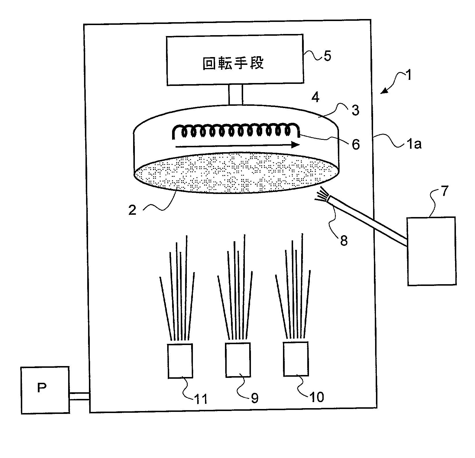
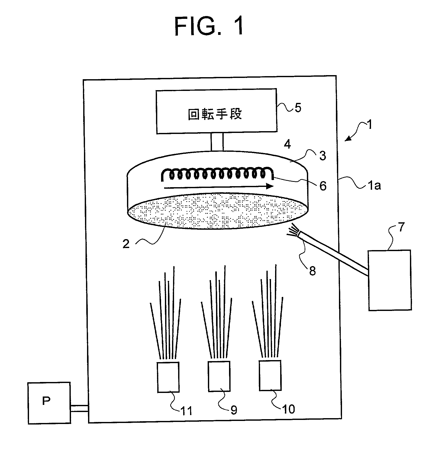
[0001] 1. Art Field[0002] The present invention relates to a multilayer thin film including a ferroelectric thin film and an electron device comprising such a multilayer thin film. Typically, the multilayer thin film may be applied to semiconductor memories, thin-film ferroelectric devices such as infrared sensors, recording media for recording information by polarization reversal of ferroelectrics by AFM (atomic force microscope) probes or the like, thin-film vibrators, thin-film VCOs and thin-film filters used for mobile communications equipment, thin-film piezoelectric devices used for liquid injectors or the like.[0003] 2. Background Art[0004] Electronic devices comprising dielectric films, ferroelectric films, piezoelectric films or the like formed and packed on Si substrates or semiconductor crystal substrates have been invented and intensively studied. For instance, LSIs having ever higher packing densities and dielectric separated LSIs using SOI technologies have been invent...
Claims
Login to View More Application Information
Patent Timeline
 IPC IPC(8): C30B23/02C30B25/02
CPCC30B23/02C30B25/02Y10T428/2495C30B29/22
InventorNOGUCHI, TAKAOYANO, YOSHIHIKOSAITOU, HISATOSHIABE, HIDENORI
OwnerSNAPTRACK