

Semiconductor device and method of manufacturing the same
a semiconductor and capacitor technology, applied in semiconductor devices, capacitors, electrical equipment, etc., can solve the problems of deformation of ferroelectric capacitor characteristics, deformation of capacitor moisture, and compressive stress of interlayer insulating film deformation
- Summary
- Abstract
- Description
- Claims
- Application Information
AI Technical Summary
Benefits of technology
Problems solved by technology
Method used
Image

Examples
first embodiment
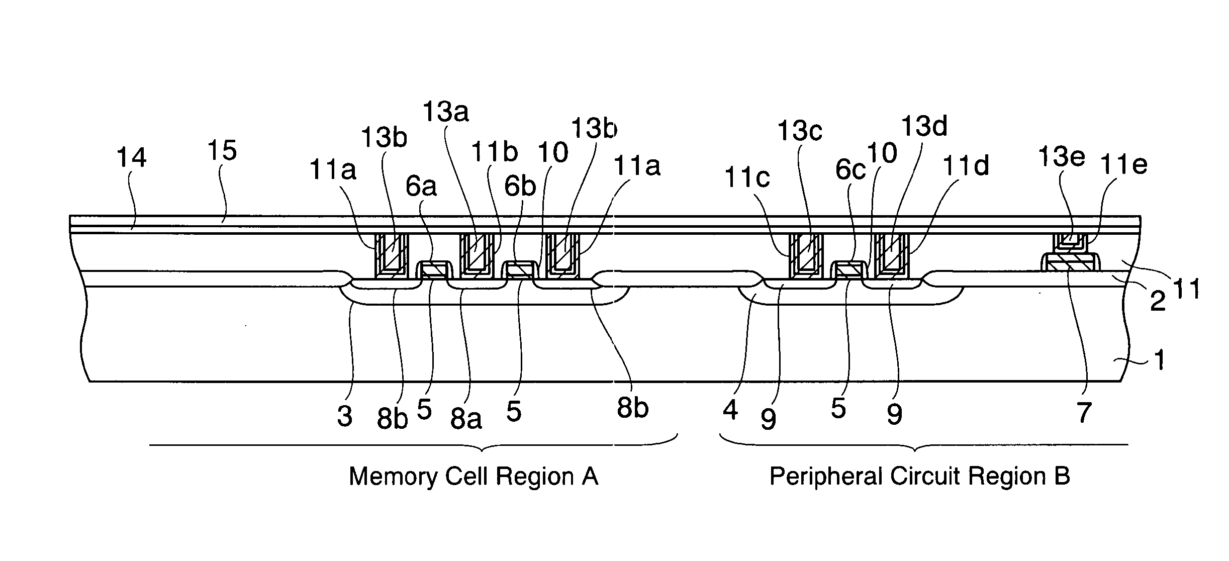
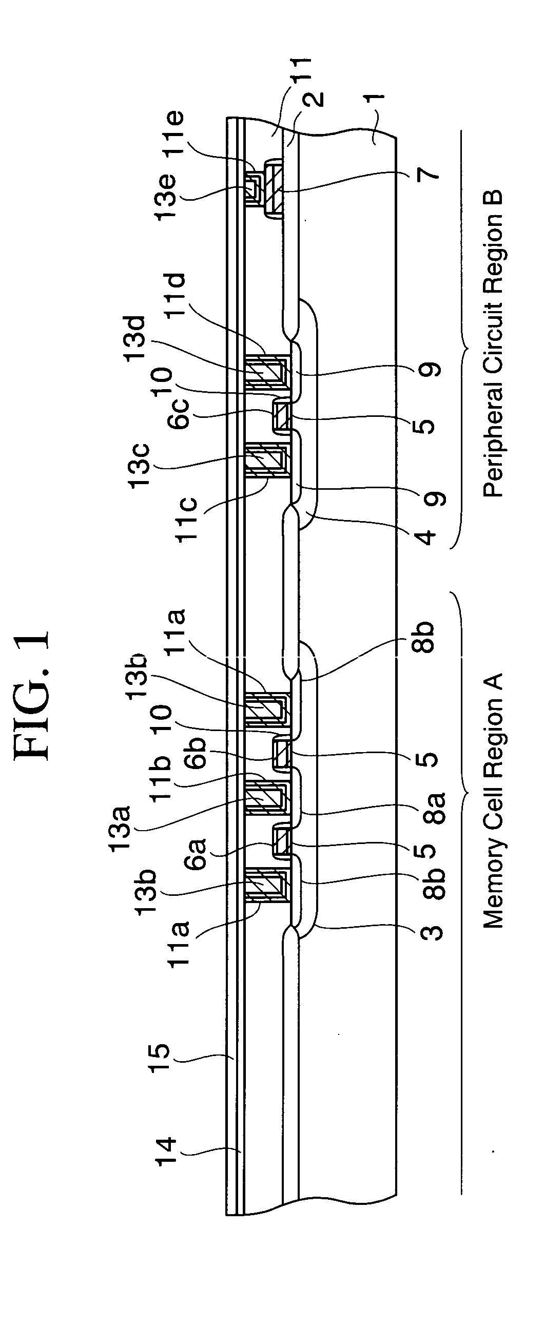
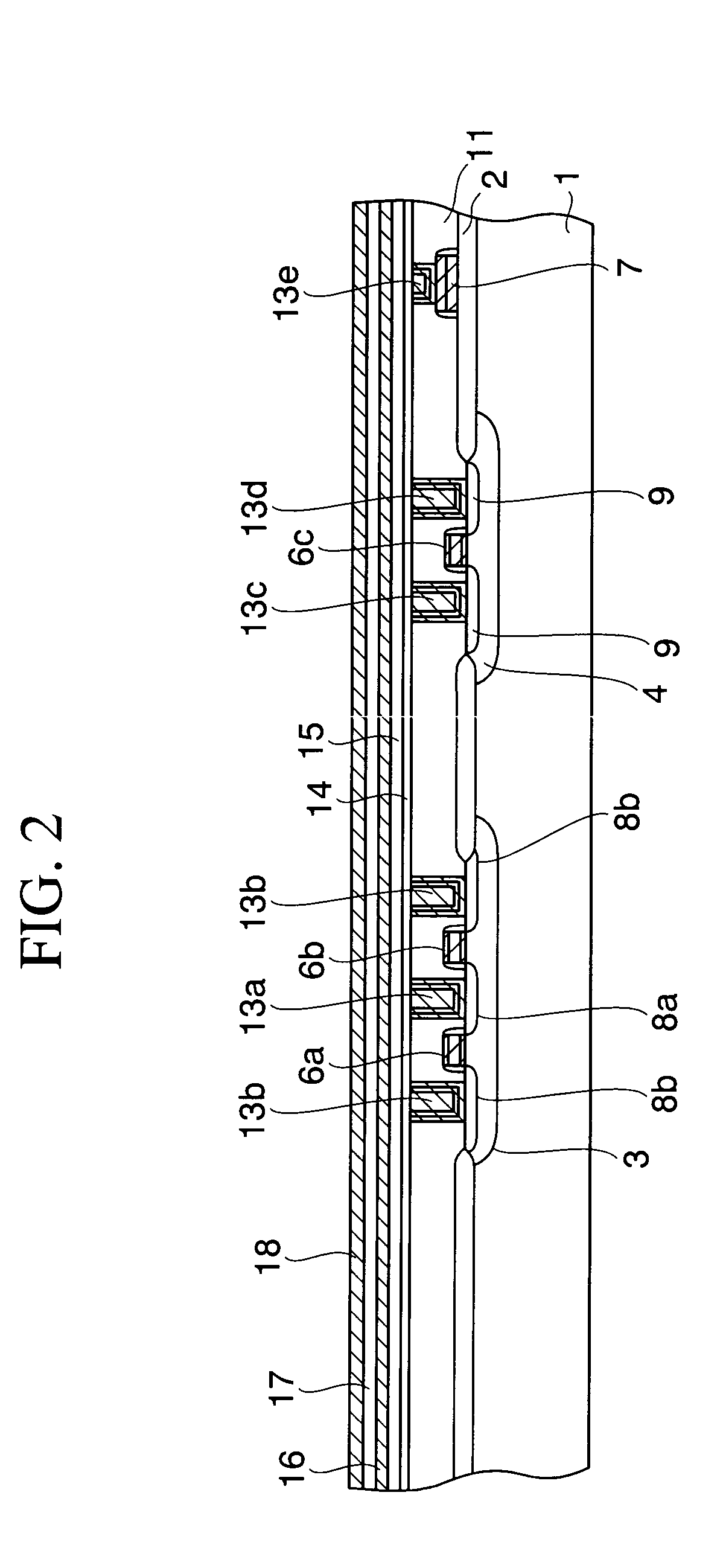
[0030] FIGS. 1 to 13 are sectional views showing a method of manufacturing semiconductor device according to the present invention in order of step. FIG. 14 is a plan view showing the semiconductor device in FIG. 13.
[0031] First, steps for forming the structure shown in FIG. 1 will be explained.
[0032] As shown in FIG. 1, LOCOS (Local Oxidation of Silicon) is formed as an element isolation insulating film 2 on a part of a surface of a p-type silicon (semiconductor) substrate 1. Another element isolation structure may be employed in place of the insulating film 2, such as STI (Shallow Trench Isolation).
[0033] After the element isolation insulating film 2 is formed, a p-well 3 and an n-well 4 are formed by selectively introducing the p-type impurity and the n-type impurity into the predetermined active regions in a memory cell region A and a peripheral circuit region B of the silicon substrate 1. It should be noted that p-well is also formed in the peripheral circuit regions for formin...
second embodiment
[0101] The present invention can be applied to the damascene process. Such application of the present invention will be explained hereunder.
[0102] FIGS. 18A to FIG. 32 are sectional views showing a manufacturing method of a semiconductor device according to a second embodiment of the present invention in order of step. In this embodiment, a stacked FeRAM will be explained hereunder. But the present invention is not limited to this embodiment, and can be applied to the planar FeRAM.
[0103] First, steps required until a sectional structure shown in FIG. 18A is formed will be explained hereunder.
[0104] As shown in FIG. 18A, an element isolation recess is formed around the transistor forming region of an n-type silicon (semiconductor) substrate 51 by the photolithography method, and then an STI element isolation insulating film 52 is formed by burying silicon oxide (SiO.sub.2) in the recess. In this case, the insulating film formed by the LOCOS method may be employed as the element isola...
PUM
 Abstract
Description
Claims
Application Information