Semiconductor device, and method of manufacturing multilayer wiring board and semiconductor device

a semiconductor and multi-layer technology, applied in the direction of dielectric characteristics, conductive pattern formation, thermoplastic polymer dielectrics, etc., can solve the problems of significant reduction in yield, significant difference in thermal expansion coefficient between semiconductor chips and multi-layer wiring boards, and conventional semiconductor packages using lead frames are approaching their limits of miniaturization, so as to prevent cracks effectively, reduce stress applied to these bumps, and prevent cracks

Active Publication Date: 2010-06-10
PANASONIC CORP
View PDF7 Cites 41 Cited by
  • Summary
  • Abstract
  • Description
  • Claims
  • Application Information

AI Technical Summary

Benefits of technology

[0022]According to the second structure as described above, the first insulating layer for supporting the first connection pads, which are connected to the bumps located at positions on which the stress generated by a temperature change is particularly concentrated, is stacked on the second insulating layer for supporting the second connection pads connected to the bumps located at other positions. That is, a level difference is formed between the first connection pads and the second connection pads, and the first connection pads are located closer to the semiconductor chip than the second connection pads. Therefore, even if all the bumps have approximately the same volume, the bumps connected to the first connection pads can be formed into a more pressed and spread-out shape than the bumps connected to the second connection pads. As a result, the enlarged cross-sectional areas of the bumps connected to the first connection pads allow the stress applied to these bumps to be reduced. Accordingly, even if the bumps having approximately the same volume are used, cracks effectively can be prevented from occurring.
[0023]As described above, according to the present invention, it is possible to prevent occurrence of cracks caused by temperature changes, and thus to obtain a high reliability of connection between the semiconductor chip and the multilayer wiring board.

Problems solved by technology

Conventional semiconductor packages using lead frames are approaching their limits of miniaturization.
This method has, however, the following problem.
A fine pitch of solder bumps may cause short circuits between adjacent bumps during printing of the solder paste, which results in a significant decrease in the yield.
However, there is a significant difference in thermal expansion coefficients between the semiconductor chip and the multilayer wiring board.
Therefore, if the semiconductor chip and the multilayer wiring board are subjected to a significant temperature change during or after the flip chip bonding, a stress is concentrated on the solder bumps serving as connecting members between the semiconductor chip and the multilayer wiring board, which may cause cracks in the solder bumps or in the vicinity thereof and result in a poor connection.
However, as described above, the size of solder bumps become narrower and narrower as semiconductor devices are miniaturized and the pin counts thereof increase, and accordingly a larger stress is applied on the solder bumps.
As a result, a concern arises that cracks cannot be prevented only by the protection of encapsulating the solder bumps with resin.
However, the ball mounting method, in which solder balls of the same size are mounted on pads, is not adequate to increase the volumes of only some of the solder bumps.
JP 2007-242782 A describes that a paste printing method or a paste dispensing method is suitable for realizing this concept, but these methods are not adequate to form solder bumps at a fine pitch, as described above.

Method used


Image

  • Semiconductor device, and method of manufacturing multilayer wiring board and semiconductor device
  • Semiconductor device, and method of manufacturing multilayer wiring board and semiconductor device
  • Semiconductor device, and method of manufacturing multilayer wiring board and semiconductor device

Examples


example 1

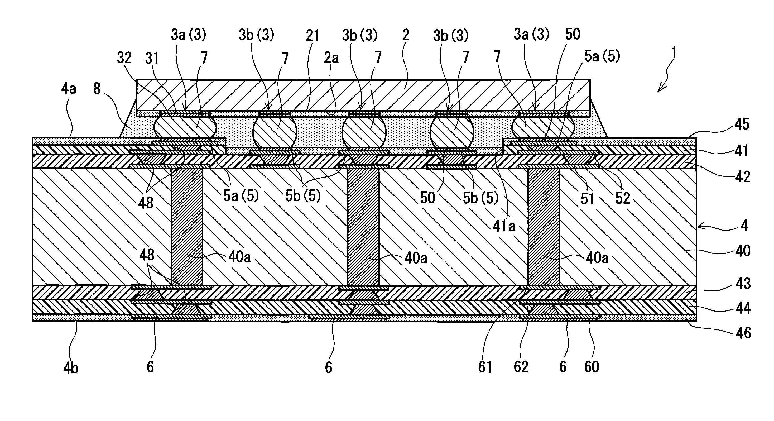
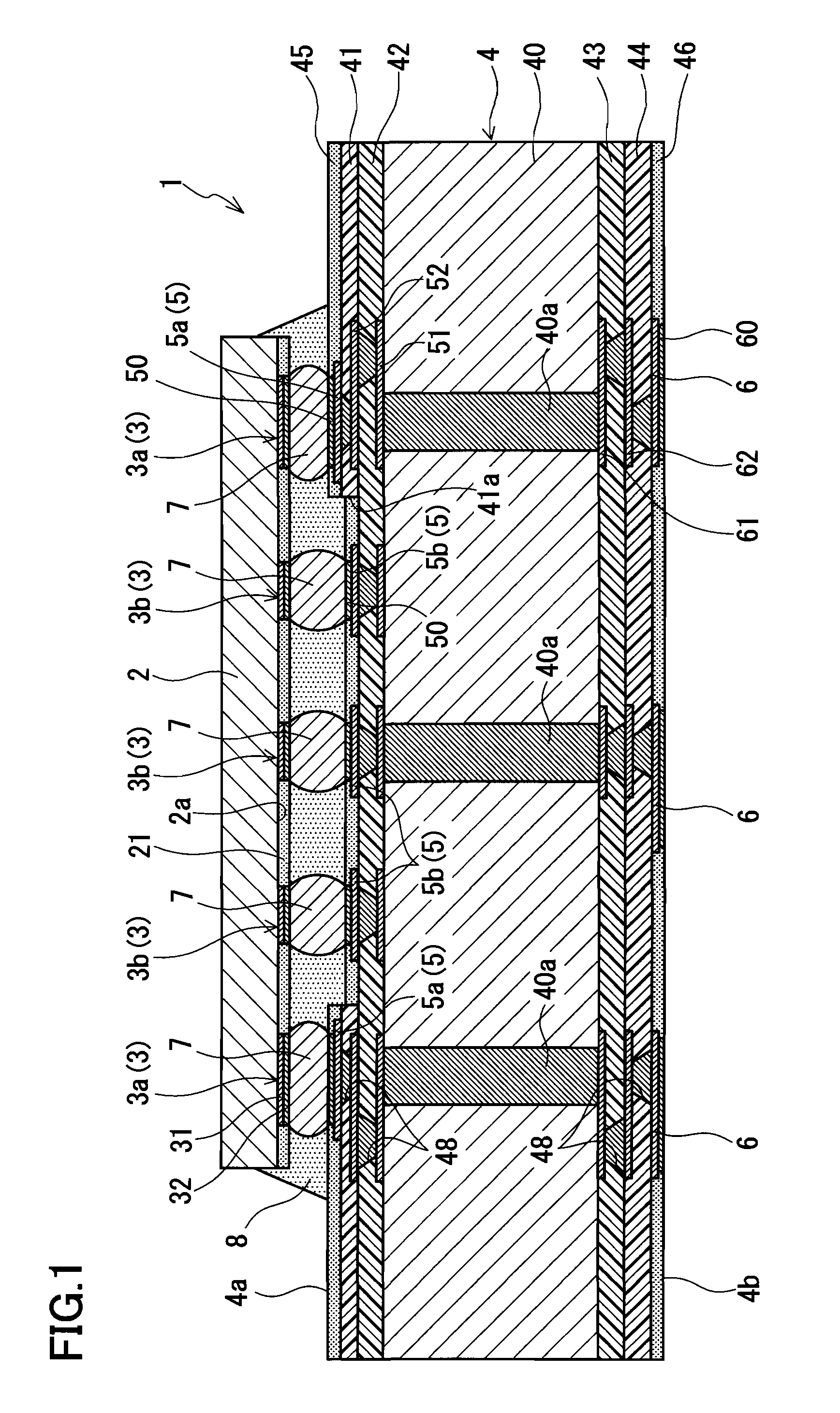
[0094]In Example 1, the semiconductor chip 2 of 8.0 mm×8.0 mm was used. The numbers of the electrode pads 3, the connection pads 5, and the solder bumps 7 were 1600 respectively (pad pitch: 180 μm). A glass epoxy substrate was used as the core substrate 40. Polyphenylene ether was used as the thermoplastic resin constituting the first insulating layer 41, and an epoxy resin containing 50 volume % of spherical silica (inorganic filler) having an average particle diameter of 5 μm was used as the thermosetting resin constituting the second insulating layer 42. The thickness of the first insulating layer 41 formed on the top surface was 30 μm, and the thickness of the second insulating layer 42 was 45 μm. As for other conditions (such as the volumes of the solder bumps 7, the shapes and sizes of the electrode pads 3 and the connection pads 5, and the sizes of the openings 45a, 45b), those specifically exemplified in the above embodiment were applied. A semiconductor device was manufactu...

example 2

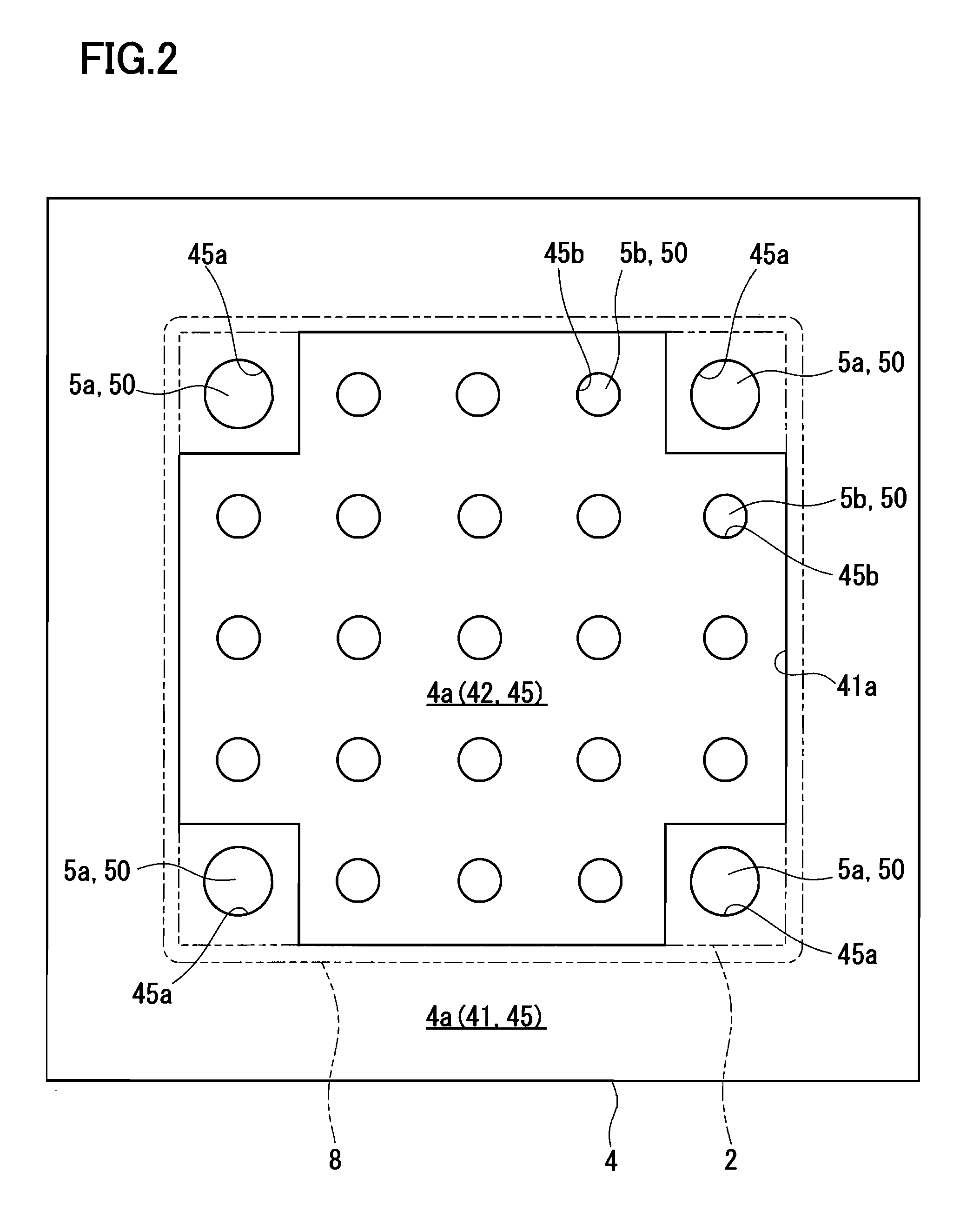
[0096]A semiconductor device was manufactured under the same conditions as those of Example 1, except that the size of the openings 45a formed at positions corresponding to the first connection pads 5a in the front-side solder resist 45 was changed from 130 μm to 90 μm of the other openings 45b.

[0097]As a result of the temperature cycle test, in the semiconductor device of Example 2, a rate of change in the connection resistance value after the 1000 cycles was +10% or less with respect to the initial resistance value. However, after the 1500 cycles, the wirings were disconnected partially. In order to identify the causes of the disconnection, a failure mode and effect analysis was carried out on the semiconductor device after being subjected to the temperature cycle test. As a result of the analysis, cracks were observed in the solder bumps 7 responsible for the disconnected wirings, and these cracks started from the points corresponding to the upper edges of the openings 45a of th...

example 3

[0098]A semiconductor device was manufactured under the same conditions as those of Example 1, except that the thickness of the first insulating layer 41 was changed to 45 μm so that the first insulating layer 41 had a thickness one half the height of the solder bumps 7 formed between the second electrode pads 3b and the corresponding second connection pads 5b.

[0099]As a result of the temperature cycle test, in the semiconductor device of Example 3, a rate of change in the connection resistance value after the 1000 cycles was +10% or less with respect to the initial resistance value. However, after the 1200 cycles, the wirings were disconnected partially. In order to identify the causes of the disconnection, a failure mode and effect analysis was carried out on the semiconductor device after being subjected to the temperature cycle test. As a result, the solder bumps 7 responsible for the disconnected wirings were pressed strongly and deformed, compared with those of Example 1, and...


PUM

PropertyMeasurementUnit
melting pointaaaaaaaaaa
thicknessaaaaaaaaaa
thicknessaaaaaaaaaa

Abstract

A semiconductor device includes a multilayer wiring board and a semiconductor chip mounted on the multilayer wiring board. Electrode pads of the semiconductor chip include: first electrode pads including electrode pads respectively disposed in the vicinity of corners of the back surface of the semiconductor chip; and second electrode pads other than the first electrode pads. Connection pads of the multilayer wiring board include: first connection pads connected to the first electrode pads via bumps; and second connection pads connected to the second electrode pads via bumps. The first connection pads are supported by a first insulating region made of a thermoplastic resin, and the second connection pads are supported by a second insulating region made of a thermosetting resin.

Description

BACKGROUND OF THE INVENTION[0001]1. Field of the Invention[0002]The present invention relates to a semiconductor device including a multilayer wiring board and a semiconductor chip mounted on the multilayer wiring board, and to a method of manufacturing the multilayer wiring board and the semiconductor device.[0003]2. Related Background Art[0004]In recent years, with the demand for higher performance and smaller size of electronic devices, higher-density integration of electronic components and even higher-density packaging thereof have been developed. Semiconductor devices (semiconductor packages) used for such electronic devices have been miniaturized and the pin counts thereof have increased more than ever before.[0005]Conventional semiconductor packages using lead frames are approaching their limits of miniaturization. In order to achieve the higher-density integration and higher-density packaging of semiconductor devices, they are fabricated using chip mounting techniques such ...

Claims


Application Information

Patent Timeline
Patent Type & Authority Applications(United States)
IPC IPC(8): H01L23/498H05K3/10H01L21/60
CPCH01L21/563Y10T29/49155H01L23/49827H01L23/49838H01L24/05H01L24/13H01L24/16H01L24/17H01L24/81H01L2224/0401H01L2224/0603H01L2224/13099H01L2224/1403H01L2224/16H01L2224/73203H01L2224/81054H01L2224/81191H01L2224/81193H01L2224/8121H01L2224/81815H01L2924/01013H01L2924/01022H01L2924/01029H01L2924/01056H01L2924/0106H01L2924/01078H01L2924/01079H01L2924/01082H05K1/0271H05K1/113H05K3/3436H05K3/4602H05K3/4688H05K2201/0129H05K2201/068H05K2201/09036H05K2201/094H05K2201/09436H05K2201/09709H05K2201/10674H05K2203/063H01L2224/0558H01L2224/05644H01L2924/01006H01L2924/01033H01L2924/01047H01L2924/0105H01L2924/01074H01L23/498H01L2224/13144H01L2224/13111H01L2224/131H01L2224/8191H01L2924/014H01L2924/00014H01L2224/16225H01L2224/16237H01L2224/17H01L2224/1703H01L2224/17051H01L2224/32225H01L2224/73204H01L2224/81011H01L2224/83385H01L2924/15787H01L2924/351H01L2924/00
Inventor HAGIHARA, KIYOMI
Owner PANASONIC CORP
Why Eureka
Try Eureka