Stage apparatus, scanning type exposure apparatus, and device produced with the same

a technology of scanning type and exposure apparatus, which is applied in the direction of photomechanical apparatus, instruments, printing, etc., can solve the problems of large wafer stage for holding the wafer, reverse deterioration of throughput, and inability to perform scanning exposure,

Inactive Publication Date: 2002-02-14
NIKON CORP
View PDF0 Cites 103 Cited by
  • Summary
  • Abstract
  • Description
  • Claims
  • Application Information

AI Technical Summary

Problems solved by technology

However, the scanning exposure is not performed during the period corresponding to the movement distance during the pre-scanning and during the over-scanning.
The elongation of the distance causes an inconvenience such that the throughput is reversely deteriorated.
Accordingly, there is such a tendency that the wafer stage for holding the wafer has a large size and a heavy weight.
Accordingly, there is such a tendency that the wafer stage necessarily has a large size and a heavy weight.
The large size and the heavy weight of the wafer stage as described above necessarily deteriorate the response performance in the positional control for the wafer stage.
For this reason, the settling time is prolonged, resulting in such an inconvenience that the throughput is reversely deteriorated although the rate of acceleration, the rate of deceleration, and the maximum velocity are originally increased in order to improve the throughput.
It has been feared that the large size of the wafer stage brings about the inconvenience such as the increase in movement area of the wafer stage, and consequently the increase in installation area for the apparatus (increase in foot print).
The inconvenience, which is involved in the large size of the stage as described above, is not limited to the exposure apparatus, and it may be caused in a similar manner in apparatuses and equipment provided with any positioning movement stage.
However, the device rule will be certainly decreased in future.
However, there is such a background that it is difficult to introduce such an apparatus due the problems that the technical hurdle is high, and the throughput is remarkably low as compared with the optical exposure apparatus.
Therefore, the time, which is required for the exposure process, is twice or more as compared with the conventional apparatus, resulting in such an inconvenience that the throughput is greatly deteriorated.
However, in the case of FIG. 29(B), the following inconvenience arises.
It is feared that the measurement of the position of the reticle stage RST may be incorrect or difficult, because of the following reason.
It is difficult to control the rotation on the side of the reticle stage RST.
If the plane mirror has a long length, it is extremely laborious to perform the accurate machining, which has caused the increase in cost as well.

Method used


Image

  • Stage apparatus, scanning type exposure apparatus, and device produced with the same
  • Stage apparatus, scanning type exposure apparatus, and device produced with the same
  • Stage apparatus, scanning type exposure apparatus, and device produced with the same

Examples


first embodiment

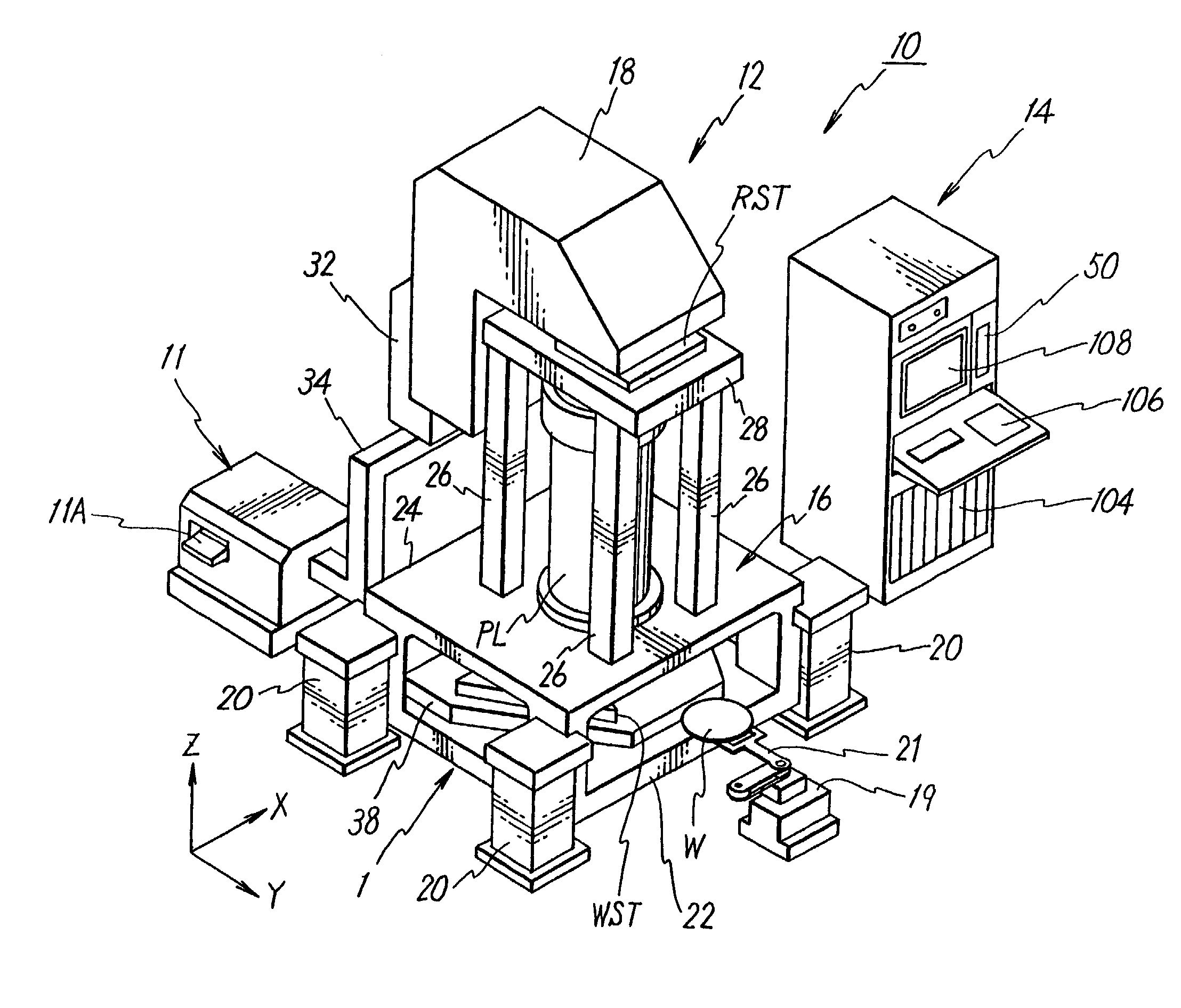
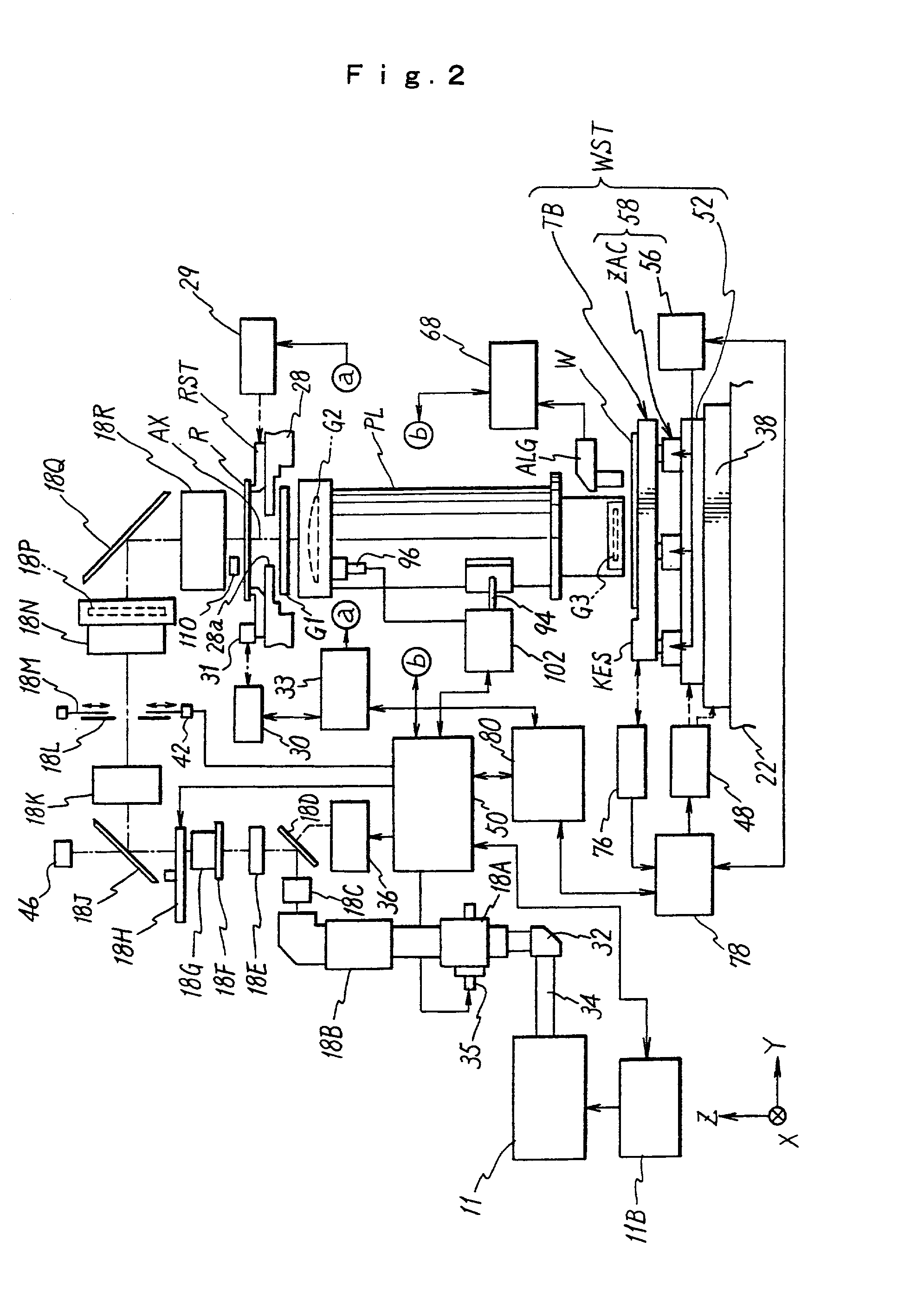
[0234] In the first embodiment, the first to fourth concepts are specified. FIG. 1 shows a perspective view illustrating a scanning type exposure apparatus 10 according to an embodiment of the present invention. FIG. 2 schematically shows an internal arrangement of the scanning type exposure apparatus 10. The scanning type exposure apparatus 10 is a projection exposure apparatus for performing the exposure operation in accordance with the step-and-scan manner which is being dominantly used as a lithography apparatus for producing semiconductor devices. The scanning type exposure apparatus 10 transfers an entire circuit pattern on a reticle R to a plurality of shot areas on a wafer W respectively in accordance with the step-and-scan manner by relatively scanning the reticle and the wafer W in the one-dimensional direction (Y direction in this case) with respect to the field of a projection optical system PL while projecting a part of the circuit pattern depicted on the reticle R as t...

second embodiment

[0461] Next, the second embodiment of the present invention will be explained with reference to FIGS. 21 to 25. The second embodiment especially discloses the second to fifth concepts of the present invention.

[0462] FIG. 21 shows a schematic arrangement of an exposure apparatus 110 according to the second embodiment. The same components as those of the first embodiment described above or components equivalent thereto are designated by the same reference numerals, explanation of which will be simplified or omitted. The exposure apparatus 100 is a projection exposure apparatus based on the so-called step-and-scan manner.

[0463] The exposure apparatus 110 comprises, for example, a stage apparatus 101 which is provided with two square wafer stages WST1, WST2 as the first movable members for making movement in the two-dimensional direction while independently holding wafers W1, W2 as the substrate respectively, a projection optical system PL which is arranged over the stage apparatus 101,...


PUM

PropertyMeasurementUnit
sizeaaaaaaaaaa
widthaaaaaaaaaa
widthaaaaaaaaaa

Abstract

An exposure apparatus has a triangular shaped stage which is movable in a two-dimensional plane while holding a substrate. The stage has a reflecting surface provided on a side face of the stage so that the surface extends in a specific direction intersecting Y axis and X axis. An interferometer radiates a beam onto the reflecting surface to measure a position of the stage in a direction perpendicular to the specific direction. Using the measured position and an angle of the specific direction, a calculator can calculate the position of the stage on rectangular coordinate system defined by X and Y axes. The size and weight of the stage can be reduced, and the throughput of the exposure apparatus is improved.

Description

CROSS REFERENCE[0001] This application is a continuation application of International Application No. PCT / JP98 / 04223 filed on Sep. 18, 1998 and priority-based on Japanese patent applications No.9-273420, No.9-279500, No.9-293249, and No.10-226500.[0002] 1. Field of the Invention[0003] The present invention relates to a scanning type exposure apparatus and a scanning exposure method used when a circuit device such as a semiconductor circuit element and a liquid crystal display element is produced in accordance with a lithography step. In particular, the present invention relates to a scanning type exposure apparatus and an exposure method preferably used to perform scanning exposure with a large mask having a size of not less than 9 inches. The present invention also relates to a device produced with the exposure method.[0004] Especially, the present invention generally includes the following five concepts in order to achieve the common objects of the present invention as described l...

Claims


Application Information

Patent Timeline
Patent Type & Authority Applications(United States)
IPC IPC(8): G03F7/20H01L21/68
CPCG03F7/70358G03F7/707G03F7/70708G03F7/70716G03F7/70725G03F7/70766G03F7/70775H01L21/681G03F7/70258
Inventor NISHI, KENJI
Owner NIKON CORP
Why Eureka
Try Eureka