Method for manufacturing microlens substrate, microlens substrate, opposing substrate for liquid crystal panel, liquid crystal panel, and projection display apparatus

a technology of microlens and substrate, which is applied in the direction of instruments, projectors, domestic applications, etc., can solve the problem of limiting the accuracy of regulating the thickness of the resin layer 909, and achieve the effects of avoiding the risk of deteriorating the optical characteristics of the microlenses 4 and reducing the risk of deterioration of the optical characteristics of the microlenses 4 and reducing the risk of deterioration of the optical characteristics

Inactive Publication Date: 2002-02-21
SEIKO EPSON CORP
View PDF0 Cites 28 Cited by
  • Summary
  • Abstract
  • Description
  • Claims
  • Application Information

AI Technical Summary

Benefits of technology

0027] 100: non-effective lens-region
0076] By providing the spacers 5 in the non-effective lens-region 100, that is, by providing the spacers 5 outside the effective lens-region 100, a risk of causing a problem, in that the spacers 5 intercept a path of light having passed through the microlenses 4, can be avoided. In other words, by providing the spacers 5 outside the effective lens-region 100, a risk of deteriorating optical characteristics of the microlenses 4 can be avoided. Therefore, the optical characteristics of the microlenses 4 can be fully exhibited.
0077] When spacers are formed in particles, as the spacers 5 according to the present example, the adhesion property between the resin layer 9 and the outer layer 8 is prevented from deteriorating. When spacers are formed in globules, as the spacers 5, the spacers are properly prevented from overlapping each other. Therefore, the thickness of the resin layer 9 can be regulated more accurately, and non-uniformity in the thickness of the resin layer 9 can be very appropriately avoided.
0078] The average particle size of the spacers 5 can be set to substantially the same as the thickness of the resin layer 9. That is, the average particle size can be properly selected in accordance with the designed value of a thickness of the resin layer 9. Generally, the average particle size of the spacers 5 is preferably in the order of 0.1 to 100 .mu.m, and more preferably in the order of 1 to 60 .mu.m. When the average particle size is set to a value in the above ranges, the thickness of the resin layer 9 can be easily set so that emitted light passing through the microlenses 3 is focused in the vicinity of the surface of the microlens substrate 1, whereby the efficiency of light usage by using the microlens substrate 1 is improved.
0084] By thus disposing the spacers 5 in the vicinity of edges of the microlens substrate 1, the spacers 5 can be very easily disposed without deteriorating the optical characteristics of the microlenses 4. "The vicinity of the edges of the microlens substrate" can be defined with respect to an intermediate part as a reference position between the individual edges (the periphery) of the microlens substrate and the center of the microlens substrate toward the edge sides.
0087] By thus forming the spacers in a belt-shape, the thickness of the resin layer 9 can be regulated with very high accuracy, and non-uniformity in the thickness of the resin layer 9 can be very appropriately suppressed.

Problems solved by technology

However, limitation of improving accuracy in regulating the thickness of the resin layer 909 by such method has been noticed.

Method used


Image

  • Method for manufacturing microlens substrate, microlens substrate, opposing substrate for liquid crystal panel, liquid crystal panel, and projection display apparatus
  • Method for manufacturing microlens substrate, microlens substrate, opposing substrate for liquid crystal panel, liquid crystal panel, and projection display apparatus
  • Method for manufacturing microlens substrate, microlens substrate, opposing substrate for liquid crystal panel, liquid crystal panel, and projection display apparatus

Examples


example 1

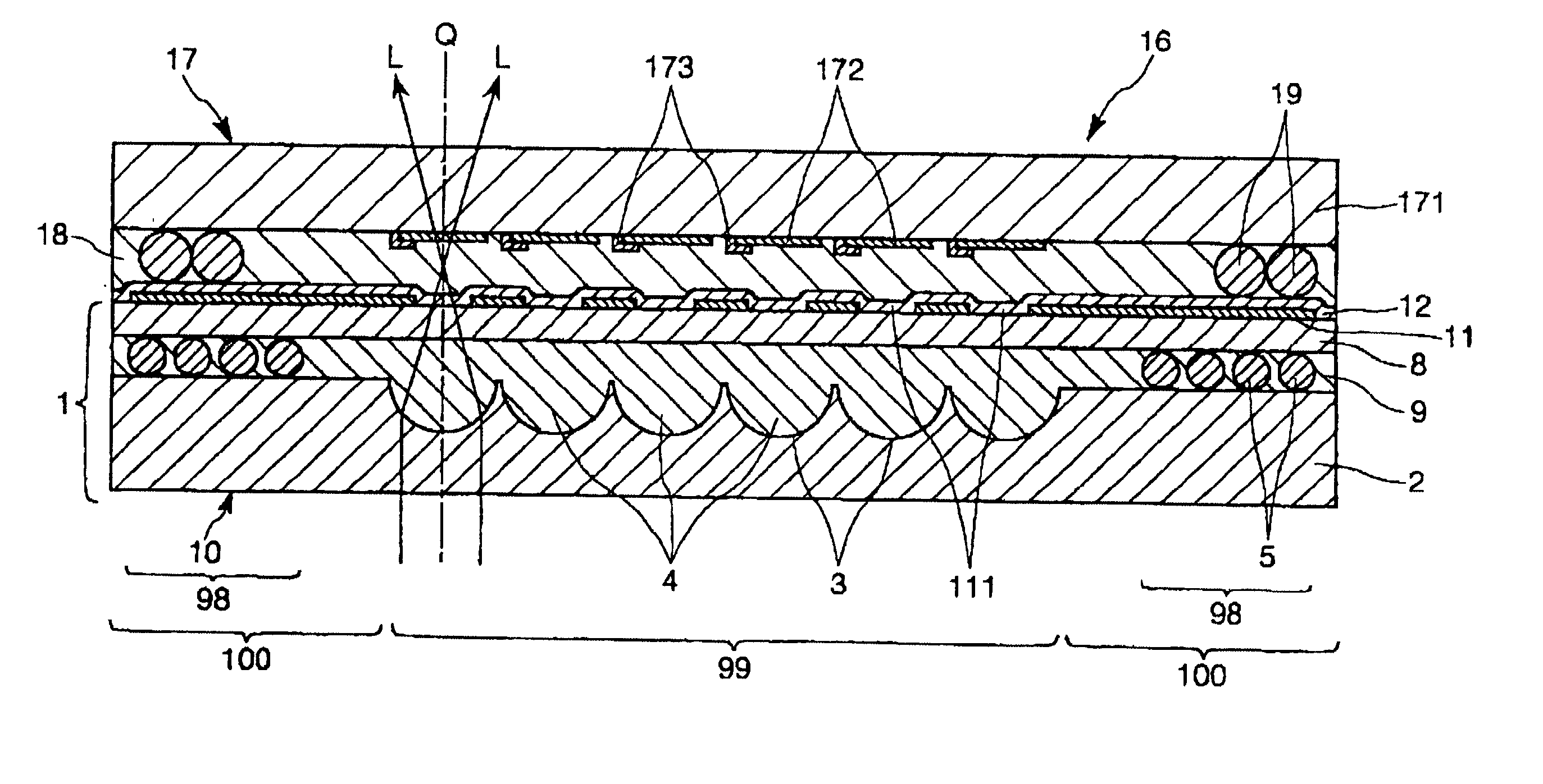
[0198] A microlens substrate was manufactured, as described below. The thickness of a resin layer was designed so as to be set to 12 .mu.m.

[0199] A green rectangular silica-glass substrate (transparent substrate) having a thickness of 1.2 mm was prepared as a base material. The silica-glass substrate was dipped in a cleaning agent (a mixture of sulfuric acid and an aqueous solution of hydrogen peroxide) so as to be cleaned, and was cleaned at the surfaces thereof.

[0200] 1. A polycrystalline silicon film having a thickness of 0.4 .mu.m was deposited by a CVD method on front and rear surfaces of the silica-glass substrate.

[0201] The deposition was performed by supplying SiH.sub.4 at a speed of 300 ml / minute to a CVD furnace which was set to 600.degree. C. and 80 Pa, in which the silica-glass substrate was placed.

[0202] 2. Openings associating with the concavities to be formed were formed in the polycrystalline silicon film.

[0203] The process was performed in a manner such that a resis...

example 2

[0212] In the same fashion as described above, a wafer-shaped microlens substrate shown in FIG. 3(i) was manufactured.

example 3

[0213] In the same fashion as described above, a wafer-shaped microlens substrate shown in FIG. 3(ii) was manufactured.

Example 4

[0214] In the same fashion as described above, a wafer-shaped microlens substrate shown in FIG. 4(iii) was manufactured.


PUM

PropertyMeasurementUnit
densityaaaaaaaaaa
particle sizeaaaaaaaaaa

Abstract

An object is to provide a microlens substrate capable of regulating the thickness of a resin layer with high accuracy. A microlens substrate 1 includes a transparent substrate 2 provided with a plurality of concavities 3 having concave surfaces, an outer layer 8 bonded to the transparent substrate 2 at a surface thereof provided with the concavities 3 via a resin layer 9, and spacers 5 for regulating the thickness of the resin layer 9. The resin layer 9 includes microlenses 4 formed with a resin filling the concavities 3. The spacers 5 include globular particles. The standard deviation of particle-size distribution of the spacers 5 is preferably not greater than 20% of an average particle size of the spacers 5. The density of the spacers 5 is preferably in the order of 0.5 to 2.0 g/cm3. A value rho1/rho2 is preferably in the order of 0.6 to 1.4, in which rho1 denotes the density (g/cm3) of the spacers 5, and rho2 denotes the density (g/cm3) of a resin forming the resin layer 9.

Description

Technical Field of the Invention[0001] The present invention relates to a method for manufacturing microlens substrate, and to a microlens substrate, an opposing substrate for a liquid crystal panel, a liquid crystal panel, and a projection display apparatus.DESCRIPTION OF THE BACKGROUND ART[0002] Hitherto, a projection display apparatus for projecting images on a screen has been known. In a projection display apparatus of this type, liquid crystal panels (liquid crystal optical shutters) are generally used for forming images.[0003] A liquid crystal panel having such a configuration is known, which is provided with a number of minute microlenses in positions, each corresponding to a pixel of the liquid crystal panel. The microlenses are generally formed on a microlens substrate provided in the liquid crystal panel.[0004] FIG. 9 is a schematic longitudinal-sectional view showing the configuration of a microlense substrate used in the known liquid crystal panel.[0005] As shown in the ...

Claims


Application Information

Patent Timeline
Patent Type & Authority Applications(United States)
IPC IPC(8): B29D11/00G02B3/00G02F1/1335G03B21/00
CPCG02B3/0025G02B3/0031G02F1/133526
Inventor YOTSUYA, SHINICHISHIMIZU, NOBUOYAMASHITA, HIDETO
Owner SEIKO EPSON CORP
Why Eureka
Try Eureka