
PLL circuit

Inactive Publication Date: 2002-03-21
NEC CORP
View PDF0 Cites 22 Cited by
  • Summary
  • Abstract
  • Description
  • Claims
  • Application Information

AI Technical Summary

Benefits of technology

[0017] Accordingly, it is an object of the present invention to provide an entirely novel PLL circuit that makes fractional frequency division possible without causing spurious signals to be produced in the output of a voltage-controlled oscillator.

Problems solved by technology

As a consequence, a problem with the prior art is that the circuitry for reducing spurious signals becomes large in scale.

Method used


Image

  • PLL circuit
  • PLL circuit
  • PLL circuit

Examples


first embodiment

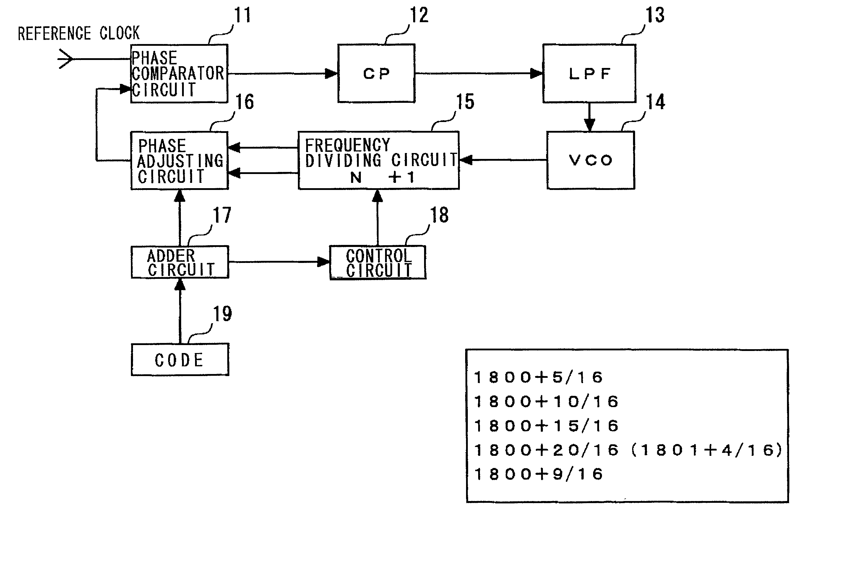
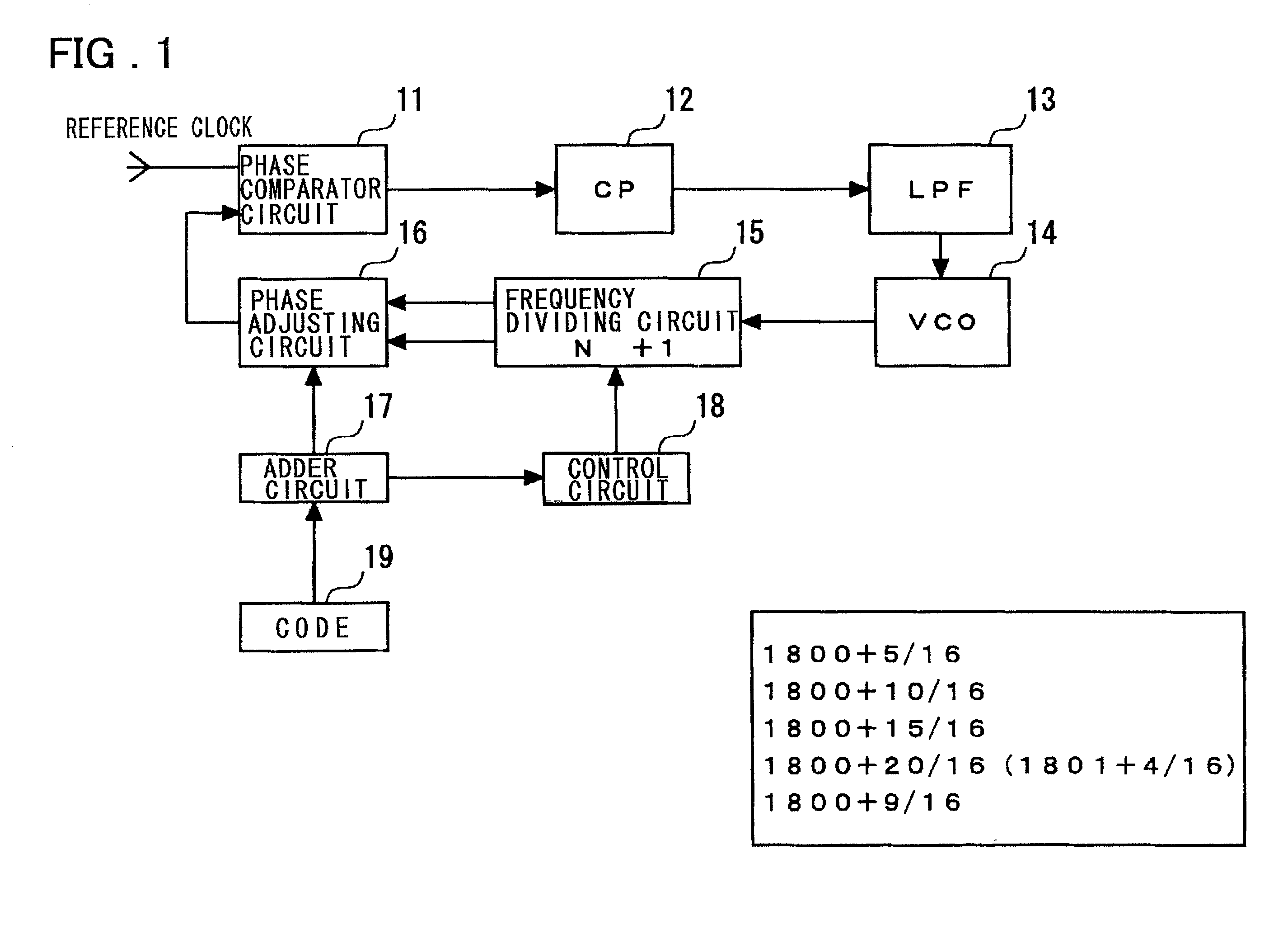
[0046] In the present invention, as shown in FIG. 1, a PLL circuit comprises: a frequency dividing circuit (15) for frequency dividing an integral part of an output signal from a voltage-controlled oscillator (14); a phase adjusting circuit (16), which receives two frequency-divided clocks of mutually different phases obtained by integral frequency division of the frequency dividing circuit(15) and generates an output signal which includes, as a delay time, a time that is the result of internally dividing a timing difference between the two frequency-divided clocks in accordance with a prescribed interior division ratio; a phase comparator circuit (11) for receiving a frequency-divided clock output from the phase adjusting circuit (16) and a reference signal to detect a phase difference between the signals received; a charge pump (12) for generating a voltage conforming to the phase difference output from the phase comparator circuit (11); and a loop filter (13) for supplying an out...

second embodiment

[0140] FIG. 9 illustrates a structure of the present invention, FIG. 10 is a diagram illustrating the connections to the interpolator portion of FIG. 9, and FIG. 11 is a diagram illustrating the timing waveforms on principal signals.

[0141] As shown in FIG. 9, the second embodiment of the invention has an interpolator 200 comprising 16-step first and second interpolators 216, 217 and a third interpolator 218 the inputs to which are the outputs of the first and second interpolators.

[0142] This embodiment includes a 16 / 17 prescaler 207 for frequency-dividing the output of a voltage-controlled oscillator 206. A signal obtained by converting a 16 / 17-divided output of the prescaler 207 to the CMOS level using an ECL / CMOS converter circuit 208 is input to an A counter 209 and to the clock input terminals of D-type flip-flops 214, 215. It should be noted that since the 16 / 17 prescaler 207, A counter 209, a B counter 210, an adder 211 and a register 212 operate in the same manner as the 32 / 3...


PUM


Abstract

Disclosed is a PLL circuit that makes fractional frequency division possible without causing spurious components to be produced in the output of a VCO. The PLL circuit comprises a frequency dividing circuit for frequency-dividing the output of a VCO; a phase adjusting circuit, to which are input two clocks of different phases obtained by frequency division performed by the frequency dividing circuit, for producing an output signal having a delay time defined by a time that is the result of internally dividing a timing difference between the two clocks; a charge pump for generating a voltage conforming to a phase difference output from the phase comparator circuit; and a loop filter for smoothing the voltage conforming to the phase difference and applying the voltage to the VCO, wherein the dividing value of the timing difference in the phase adjusting circuit is represented by MF / MD, and an accumulation operation is performed in units of MF every frequency-divided clock. If the cumulative result by MF is equal to or greater than MD, then a remainder obtained by dividing the cumulative result by MD is adopted as the cumulative result and the dividing ratio of the frequency dividing circuit is set to N+1. A control signal for setting the dividing ratio of the timing difference in the phase adjusting circuit is output to the phase adjusting circuit, and a clock obtained by frequency-dividing the output of the VCO in accordance with a dividing ratio N+MF / MD is input to a phase comparator.

Description

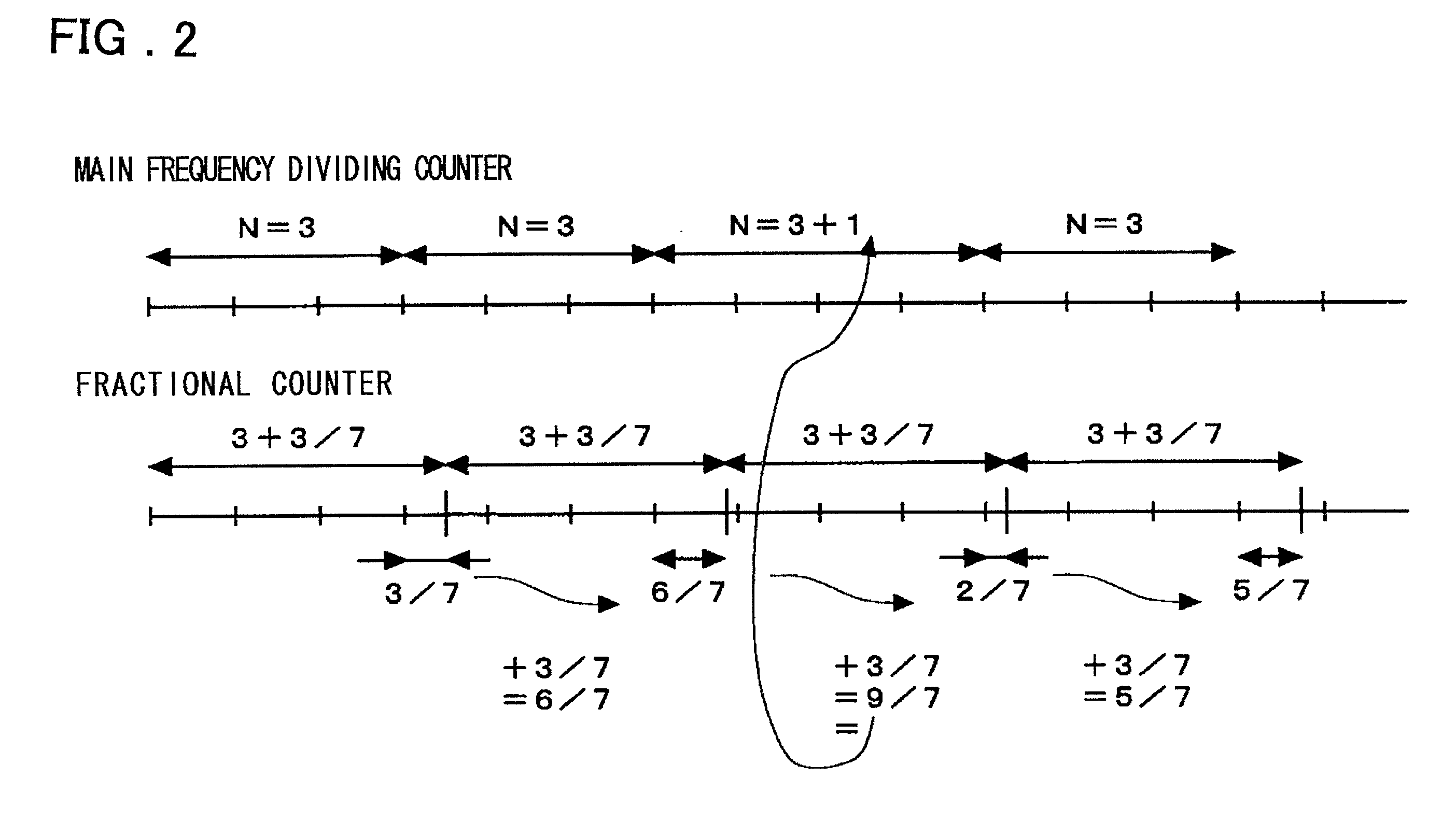
[0001] This invention relates to a phase-locked loop circuit and, more particularly, to a phase-locked loop circuit of fractional frequency-dividing type.BACKGROUND OF THE INVENITON[0002] In order to control the frequency of an output signal at a frequency interval smaller than the frequency of a reference signal, the conventional practice is to employ an arrangement which averages, in terms of time, a frequency dividing ratio of a programmable frequency dividing circuit with the frequency dividing ratio being variable in an ordinary phase-locked loop (PLL) to implement a frequency dividing ratio of an accuracy finer than a decimal-point by using the average value. A configuration in which the dividing ratio of a frequency dividing circuit is changed and averaged in terms of time to implement fractional frequency division in equivalent terms is also referred to as a fractional frequency-dividing system.[0003] If one period 1 / fr of a reference signal of which frequency is fr is adopt...

Claims


Application Information

Patent Timeline
IPC IPC(8): H03L7/183H03L7/08H03L7/081H03L7/089H03L7/197
CPCH03L7/081H03L7/0891H03L7/1978H03L7/08
Inventor SAEKI, TAKANORITANAKA, TOSHIYUKI
Owner NEC CORP
Learn More