

Optical inspection apparatus for defect detection
a technology of optical inspection apparatus and defect detection, which is applied in the direction of material analysis, instruments, television systems, etc., can solve the problems of high false alarm rate, system extremely slow, and inability to detect defects in the pattern of patterned semiconductor wafers, and achieve low false alarm rate, high throughput, and high speed
- Summary
- Abstract
- Description
- Claims
- Application Information
AI Technical Summary
Benefits of technology
Problems solved by technology
Method used
Image

Examples
Embodiment Construction
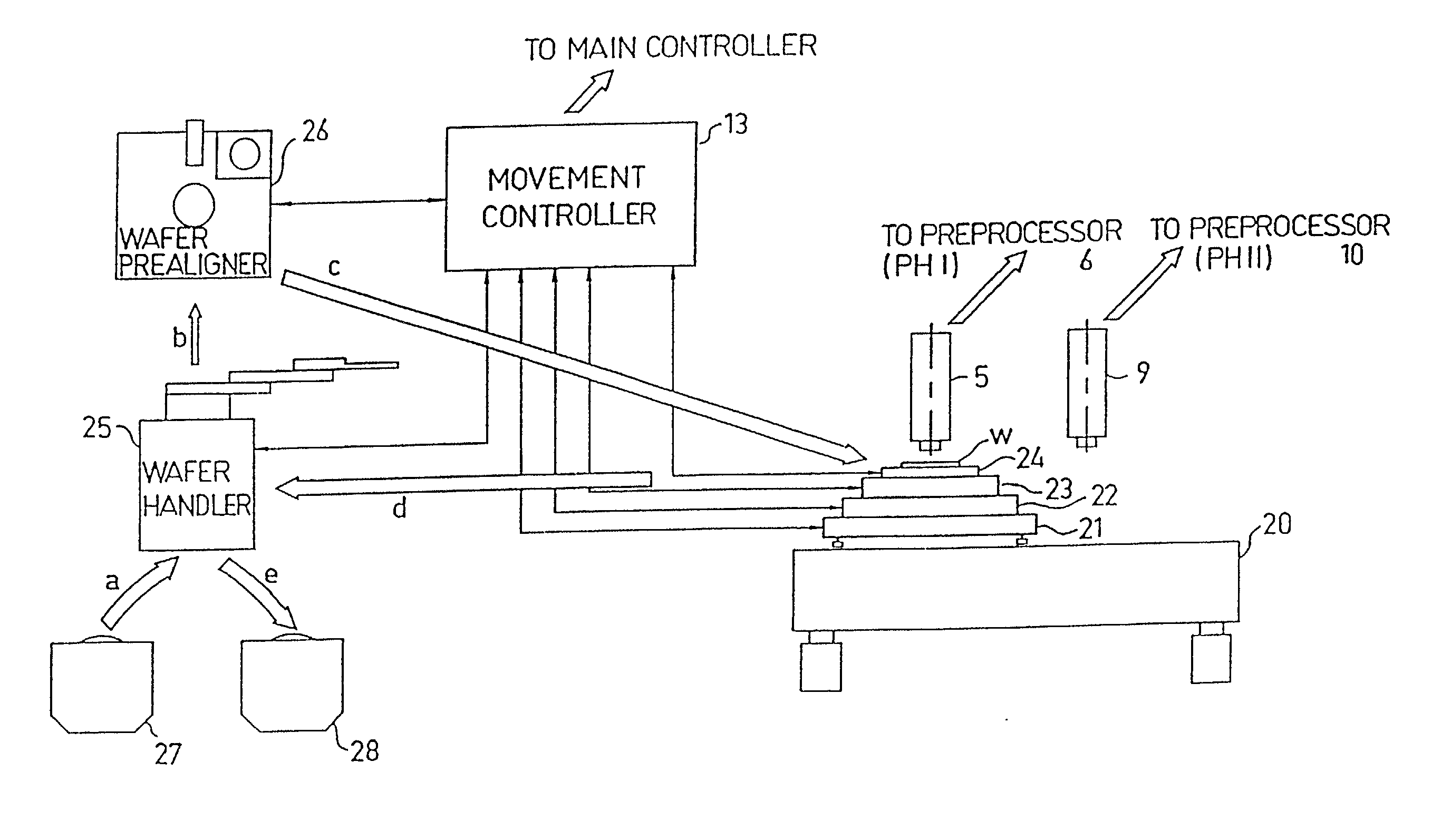
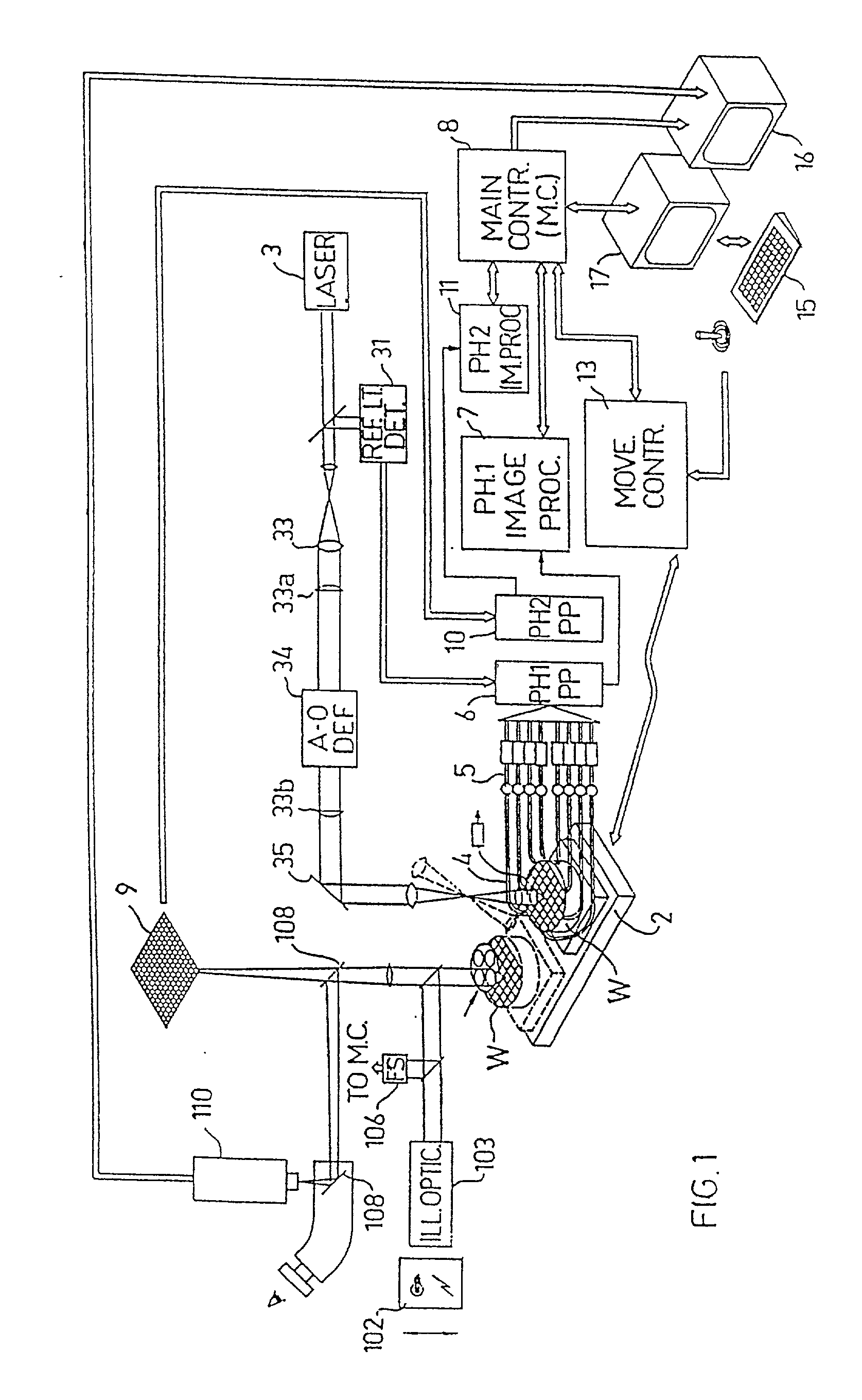
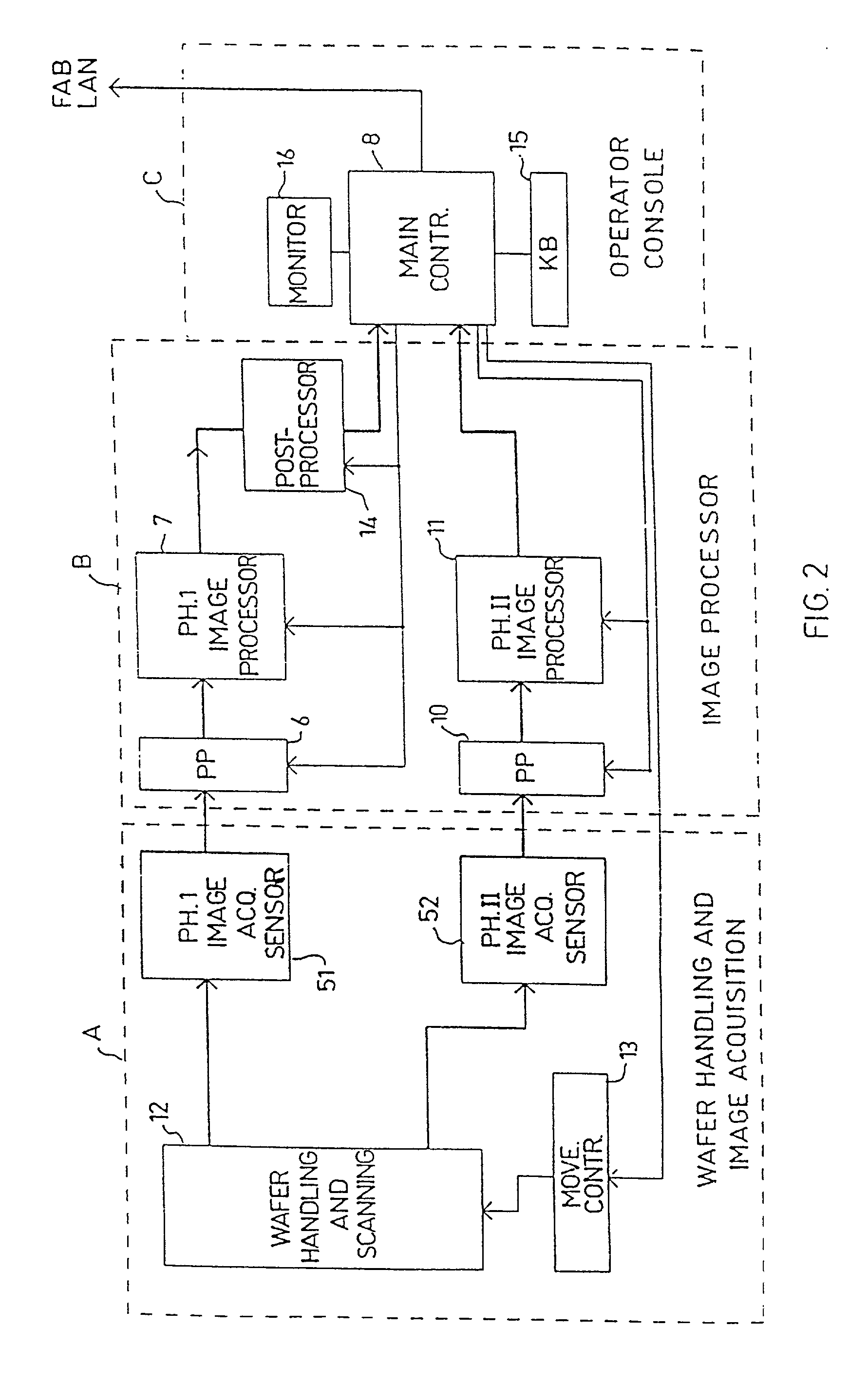
[0055] Overall System
[0056] The system illustrated in the drawings is designed particularly for automatically inspecting patterned semiconductor wafers having a plurality of like integrated-circuit dies each formed with like patterns. The system inspects each pattern, called the inspected pattern, by comparing it with at least one other pattern on the wafer, serving as the reference pattern, to detect any differences which would indicate a defect in the inspected pattern.
[0057] The inspection is made in two phases: In the first phase, the complete surface of the wafer is inspected at a relatively high speed and with a relatively low spatial resolution; and information is outputted indicating suspected locations on the wafer having a high probability of a defect. These locations are stored in a storage device. In the second phase, only the suspected locations stored in the storage device are examined with a relatively high spatial resolution; and a determination is made as to the pre...
PUM
| Property | Measurement | Unit |
|---|---|---|
| length | aaaaa | aaaaa |
| length | aaaaa | aaaaa |
| distance | aaaaa | aaaaa |
Abstract
Description
Claims
Application Information