Process for making and programming and operating a dual-bit multi-level ballistic MONOS memory

a multi-level ballistic monos and memory technology, applied in the field of dual-bit multi-level ballistic monos memory making and programming, can solve the problems of not meeting the interests of high-density memory, cumbersome peripheral logic,

Inactive Publication Date: 2002-04-18
HALO LSI INC
View PDF0 Cites 41 Cited by
  • Summary
  • Abstract
  • Description
  • Claims
  • Application Information

AI Technical Summary

Problems solved by technology

Although it is also possible to operate the memory array with individual sidewall gates as control gates, peripheral logic will become more cumbersome, which does not meet the interests of high density memory.

Method used


Image

  • Process for making and programming and operating a dual-bit multi-level ballistic MONOS memory
  • Process for making and programming and operating a dual-bit multi-level ballistic MONOS memory
  • Process for making and programming and operating a dual-bit multi-level ballistic MONOS memory

Examples


Embodiment Construction

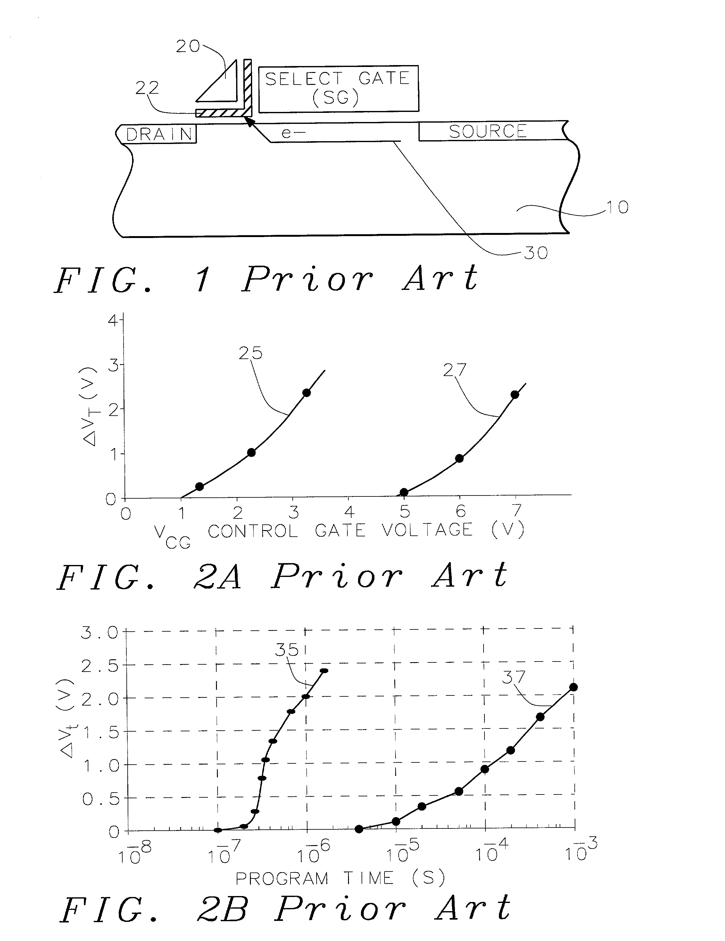
[0072] Read operation for a two bit multi-level storage in each of the nitride regions will be described, based on simulations for a 0.25u process. FIG. 8A illustrates the memory cell and voltage conditions for a read of nitride charge region 313. The threshold voltages for the four levels of storage are 0.8V, 1.2V 1.6V and 2.0 for the "11", "10", and "01" and "00" states, respectively. This is shown in FIG. 8B. The threshold voltage for the word select gate is 0.5V. During read, the source voltage is fixed to 1.2V. The control gate above the unselected nitride charge region is set to 5V, which overrides all possible threshold states, and the control gate above the selected nitride charge region is set to 2.0V, which is the highest threshold voltage of all the possible threshold states. All other control gates are set to zero, and the bit junction is precharged to zero. The word line is then raised from 0V to 1.0V, and the bit junction is monitored.

[0073] Sensing the bit junction yi...


PUM


Abstract

A fast low voltage ballistic program, ultra-short channel, ultra-high density, dual-bit multi-level flash memory is described. The structure and operation of this invention is enabled by a twin MONOS cell structure having an ultra-short control gate channel of less than 40 nm, with ballistic injection which provides high electron injection efficiency and very fast program at low program voltages of 3~5V. The ballistic MONOS memory cell is arranged in the following array: each memory cell contains two nitride regions for one word gate, and ½ a source diffusion and ½ a bit diffusion. Control gates can be defined separately or shared together over the same diffusion. Diffusions are shared between cells and run in parallel to the side wall control gates, and perpendicular to the word line. The features of fast program, low voltage, ultra-high density, dual-bit, multi-level MONOS NVRAM of the present invention include: 1) Electron memory storage in nitride regions within an ONO layer underlying the control gates, 2) high density dual-bit cell in which there are two nitride memory storage elements per cell, 3) high density dual-bit cell can store multi-levels in each of the nitride regions, 4) low current program controlled by the word gate and control gate, 5) fast, low voltage program by ballistic injection utilizing the controllable ultra-short channel MONOS, and 6) side wall control poly gates to program and read multi-levels while masking out memory storage state effects of the unselected adjacent nitride regions and memory cells.

Description

[0001] 1) Field of Invention[0002] The invention relates to methods of forming high-density Metal / polysilicon Oxide Nitride Oxide Silicon (MONOS) memory arrays and the resulting high density MONOS memory arrays.[0003] 2) Description of Prior Art[0004] Floating gate and MONOS are two types of non-volatile memories. In conventional floating gate structures, electrons are stored onto a floating gate, by either F-N tunneling or source side injection. Conventional MONOS devices store electrons usually by direct tunneling in the Oxide-Nitride-Oxide (ONO) layer which is below the memory word gate. Electrons are trapped in the Nitride layer of the ONO composite. The MONOS transistor requires one less polysilicon layer than the floating gate device, which simplifies the process and could result in a denser array.[0005] MONOS structures are conventionally planar devices in which an ONO composite layer is deposited beneath the word gate. The thickness of the bottom oxide of the ONO layer is re...

Claims


Application Information

Patent Timeline
Patent Type & Authority Applications(United States)
IPC IPC(8): G11C11/56G11C16/04H01L21/8246H01L27/115
CPCG11C11/5671H01L27/11568H01L27/115G11C16/0475H10B43/30H10B69/00
Inventor OGURA, SEIKIHAYASHI, YUTAKAOGURA, TOMOKO
Owner HALO LSI INC
Why Eureka
Try Eureka