

Three dimensional device integration method and integrated device
a technology of integrated devices and semiconductors, applied in semiconductor devices, solid-state devices, basic electric elements, etc., can solve the problems of minimum size needed, physical limits of the density which can be achieved in 2-d, and significant increase in interconnection requirements between components
- Summary
- Abstract
- Description
- Claims
- Application Information
AI Technical Summary
Benefits of technology
Problems solved by technology
Method used
Image

Examples
example
[0077] An example of the bonding between multiple devices is shown in FIGS. 11A, 11B and 12-15. FIGS. 11A, 11B and 12-15 illustrate how the bonding according to the present invention can be used to integrate N 2D arrays of devices, how they can be interconnected to form a vertically-integrated multi-wafer module, and how different technologies may be joined.
[0078] FIGS. 11A and 11B illustrate two devices to be bonded. In this example, the devices of FIGS. 11A and 11B are dissimilar integrated circuit wafers having interconnections. In FIG. 11A a symmetric-intrinsic HBT (SIHBT) wafer contains an SIHBT surrogate substrate 40, planarizing material 41 formed on substrate 40, SIHBT device 43 and interconnects 42 and 44, preferably formed of a metal. FIG. 11B illustrates a VCSEL device having a VCSEL substrate 45, planarizing material 46, VCSEL device 48 and interconnects 47 and 49, again preferably formed of metal. As shown in FIG. 12, the devices of FIGS. 11A and 11B are bonded in the m...
first embodiment
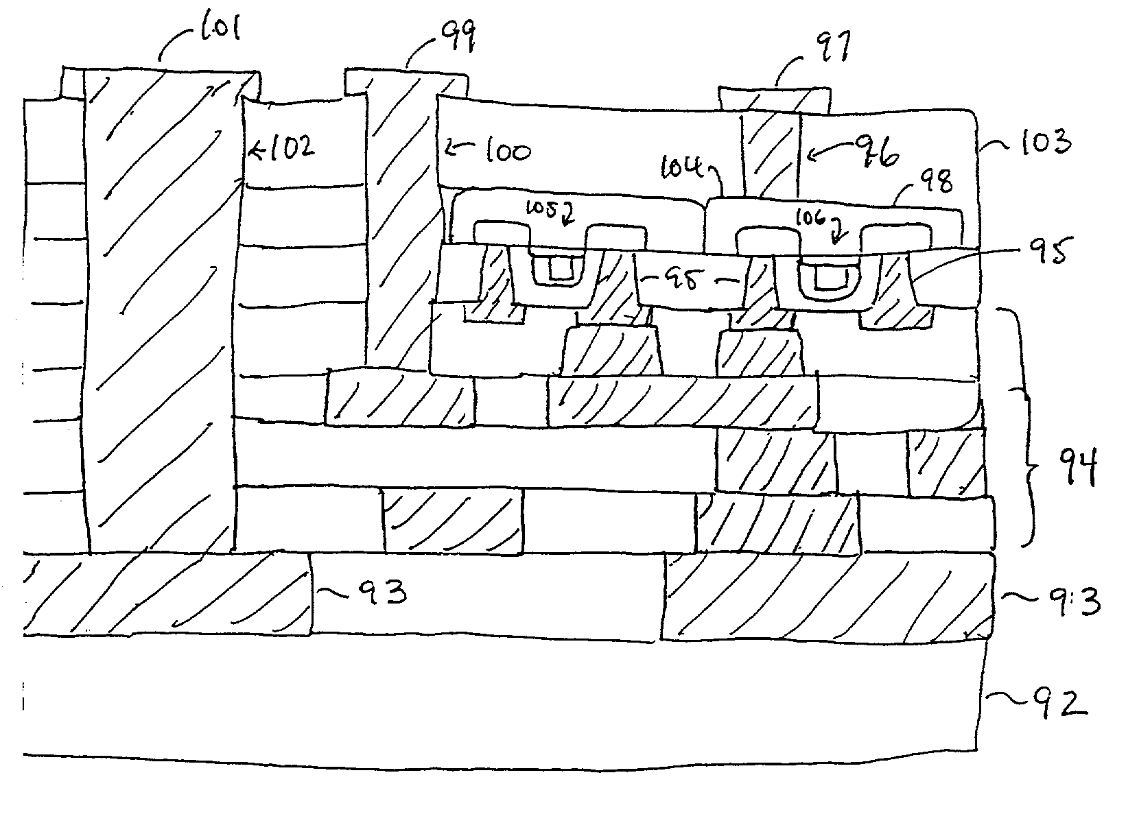
[0083] The bonding of a third wafer to the structure of FIG. 14 is illustrated in FIG. 15. It is noted that FIG. 15 illustrates an additional metalization 53 formed by etching planarizing material 41 and 46 to expose a portion of interconnect 60 of another device having elements 60-62. Interconnect 53 has an extended portion on the surface of planarizing material 41 to facilitate interconnection on another level. The device in the third wafer in this case can be a CMOS device 56 having interconnects 55 and 57. Another via is etched through planarizing material 58 and through bonding material 52, exposing a portion of interconnect 51 to allow connection with interconnect 59. Interconnect 59 is also connected with interconnect 55 of CMOS device 56. Another interconnect 54 is formed by etching a via through materials 58 and 52 to expose a portion of interconnect 53. An interconnect 54 is formed to contact interconnect 53. It should be noted that FIG. 15 does not explicitly show the bon...
fourth embodiment
[0091] the invention uses the techniques described above to create the interconnect separately from the underlying integrated circuit. Typically, circuits require a number of levels of interconnect in order to provide all the complex functions required. Six or more levels of interconnect may be needed. This requires a significant amount of thermal processing, exposing the underlying active devices to higher thermal budgets and complicating the fabricating process. The present invention may be used to fabricate the active devices separately and then forming layers of interconnect by bonding according to the present invention. In particular, each level of interconnect may be formed on separate substrates, then bonded together and interconnected as needed. Several or all of the interconnect layers may be fabricated at one time. The bonded together or single interconnected substrate may then be bonded to the substrate having the active devices. Techniques similar to those described abov...
PUM
 Abstract
Description
Claims
Application Information