Three dimensional integrated device

a semiconductor and three-dimensional technology, applied in the direction of solid-state devices, transistors, basic electric elements, etc., can solve the problems of reducing the interconnection density of components, and limiting the density of 2-d, etc., to achieve high integration density.

Inactive Publication Date: 2005-06-14
INVENSAS BONDING TECH INC
View PDF63 Cites 33 Cited by
  • Summary
  • Abstract
  • Description
  • Claims
  • Application Information

AI Technical Summary

Benefits of technology

[0011]It is an object of the present invention to provide a method and device having high integration density.
[0015]It is a still further object of the invention to avoid or minimize the thermal budgets in interconnecting devices.

Problems solved by technology

Although dramatic improvements in lithography have resulted in considerable improvement in this 2-D integration, there are physical limits to the density which can be achieved in 2-D.
One of these limits is simply the minimum size needed to make these components.
Another limit is the significant increase in interconnect requirements between components as the component size is reduced.
Although this potentially results in more components per chip area, it suffers from other problems including significantly increased thermal budgets.
Another problem results from the lagging of the ability to scale interconnect dimensions compared to scaling device dimensions.
However, since the scaling of vias lags the scaling of devices, integration density is limited.
Further problems arise when trying to integrate different types of technologies into a single circuit or wafer.
Processes required for one technology often interfere with processes required for another.
As a result, compromises are made.
The overall development of the combined technology becomes frozen in time, making flexible integration of the technologies that are being combined very difficult if not impossible.
In other words, the most advanced “best of breed” technologies are not combined and evolutions in the technologies cannot be exploited.
Another problem of combining technologies is that customization must occur up front.
One must first design the processing to combine the technologies and thus the limitations are built into the device.
Again, one cannot easily take advantage of evolutions and improvements in technology since that requires redesigning the processing.

Method used


Image

  • Three dimensional integrated device
  • Three dimensional integrated device
  • Three dimensional integrated device

Examples


example

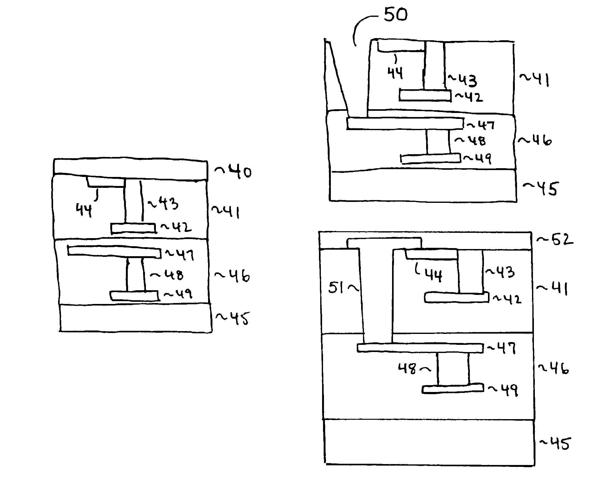
[0077]An example of the bonding between multiple devices is shown in FIGS. 11A, 11B and 12-15. FIGS. 11A, 11B and 12-15 illustrate how the bonding according to the present invention can be used to integrate N 2D arrays of devices, how they can be interconnected to form a vertically-integrated multi-wafer module, and how different technologies may be joined.

[0078]FIGS. 11A and 11B illustrate two devices to be bonded. In this example, the devices of FIGS. 11A and 11B are dissimilar integrated circuit wafers having interconnections. In FIG. 11A a symmetric-intrinsic HBT (SIHBT) wafer contains an SIHBT surrogate substrate 40, planarizing material 41 formed on substrate 40, SIHBT device 43 and interconnects 42 and 44, preferably formed of a metal. FIG. 1B illustrates a VCSEL device having a VCSEL substrate 45, planarizing material 46, VCSEL device 48 and interconnects 47 and 49, again preferably formed of metal. As shown in FIG. 12, the devices of FIGS. 11A and 11B are bonded in the meth...


PUM

PropertyMeasurementUnit
dielectric constantaaaaaaaaaa
relative dielectric constantsaaaaaaaaaa
surface roughnessaaaaaaaaaa

Abstract

A device integration method and integrated device. The method includes the steps of polishing surfaces of first and second workpieces each to a surface roughness of about 5-10 Å. The polished surfaces of the first and second workpieces are bonded together. A surface of a third workpiece is polished to the surface roughness. The surface of the third workpiece is bonded to the joined first and second workpieces. The first, second and third workpieces may each be a semiconductor device having a thin material formed on one surface, preferably in wafer form. The thin materials are polished to the desired surface roughness and then bonded together. The thin materials may each have a thickness of approximately 1-10 times the surface non-planarity of the material on which they are formed. Any number of devices may be bonded together, and the devices may be different types of devices or different technologies.

Description

BACKGROUND OF THE INVENTION[0001]1. Field of the Invention[0002]The present invention relates to three-dimensionally integrated semiconductor devices and, in particular, to semiconductor devices vertically bonded together to form three-dimensional structures.[0003]2. Discussion of the Background[0004]The ability to integrate determines the success of the semiconductor industry. This was first demonstrated with the invention of the integrated circuit (IC). The IC essentially consists of fabrication of electronic components at the surface of the semiconductor wafer followed by interconnection of these components with metalization on top of the components. The dramatic reduction in cost and increase in performance that has resulted from this integration has had a profound economic impact.[0005]Since the invention of the IC, the semiconductor industry has experienced continued rapid growth due to continuous improvements in the integration density of various electronic components (i.e., ...

Claims


Application Information

Patent Timeline
Patent Type & Authority Patents(United States)
IPC IPC(8): H01L21/70H01L21/98H01L21/331H01L21/02H01L21/20H01L21/60H01L21/768H01L21/822H01L21/8234H01L21/8238H01L27/00H01L27/04H01L27/088H01L27/092H01L29/737
CPCH01L21/2007H01L21/6835H01L21/76898H01L21/8221H01L23/13H01L23/36H01L23/481H01L23/5389H01L24/24H01L24/26H01L24/80H01L24/82H01L24/83H01L24/94H01L25/0652H01L25/0655H01L25/0657H01L25/16H01L25/167H01L25/50H01L23/552H01L25/18H01L27/14634H01L2221/6835H01L2221/68359H01L2221/68363H01L2223/6677H01L2224/1134H01L2224/16H01L2224/24011H01L2224/24225H01L2224/24226H01L2224/24227H01L2224/48091H01L2224/48101H01L2224/48227H01L2224/48247H01L2224/81894H01L2224/8319H01L2224/8385H01L2224/83894H01L2224/9202H01L2225/06513H01L2225/06541H01L2225/06589H01L2924/01015H01L2924/01029H01L2924/01047H01L2924/01057H01L2924/01074H01L2924/01082H01L2924/07802H01L2924/10329H01L2924/13091H01L2924/14H01L2924/15153H01L2924/15165H01L2924/19041H01L2924/19043H01L2924/30105H01L2924/30107H01L2924/3011H01L2924/3025H01L2924/13063H01L24/48H01L2924/00013H01L2924/01005H01L2924/01006H01L2924/01033H01L2924/014H01L2924/0132Y10S148/012Y10S438/977H01L2924/10253H01L2924/13064H01L2924/13062H01L2924/1461H01L2924/1305H01L2924/00014H01L2224/13099H01L2924/01049H01L2924/01031H01L2924/00H01L2224/24H01L2224/24051H01L2224/24145H01L2224/24146H01L2224/48H01L2224/73265H01L2224/80896H01L2224/9212H01L2224/94H01L2924/351H01L2224/45099H01L2224/45015H01L2924/207H01L2224/8203H01L2224/821H01L2224/80001H01L2224/82H01L2924/00012H01L25/00H01L21/187H01L21/76251H01L23/5384H01L23/5385H01L24/08H01L24/27H01L24/30H01L27/0688H01L2224/0807H01L2224/08123H01L2224/3005H01L2224/30104H01L2224/305H01L2224/8303H01L2224/83092H01L2224/83099H01L2224/83193H01L2224/83345H01L2224/83359H01L2224/83896H01L2224/83912H01L2224/83948H01L2225/06524H01L2225/06555H01L2924/05442
Inventor ENQUIST, PAUL M.
Owner INVENSAS BONDING TECH INC
Why Eureka
Try Eureka