Lead frame and semiconductor package
a technology of lead frame and semiconductor package, which is applied in the direction of semiconductor device details, semiconductor/solid-state device devices, electrical apparatus, etc., can solve the problems of peeling between layers, increase in cost factor, and labor costs for measuring the size of the plating area
- Summary
- Abstract
- Description
- Claims
- Application Information
AI Technical Summary
Problems solved by technology
Method used
Image

Examples
Embodiment Construction
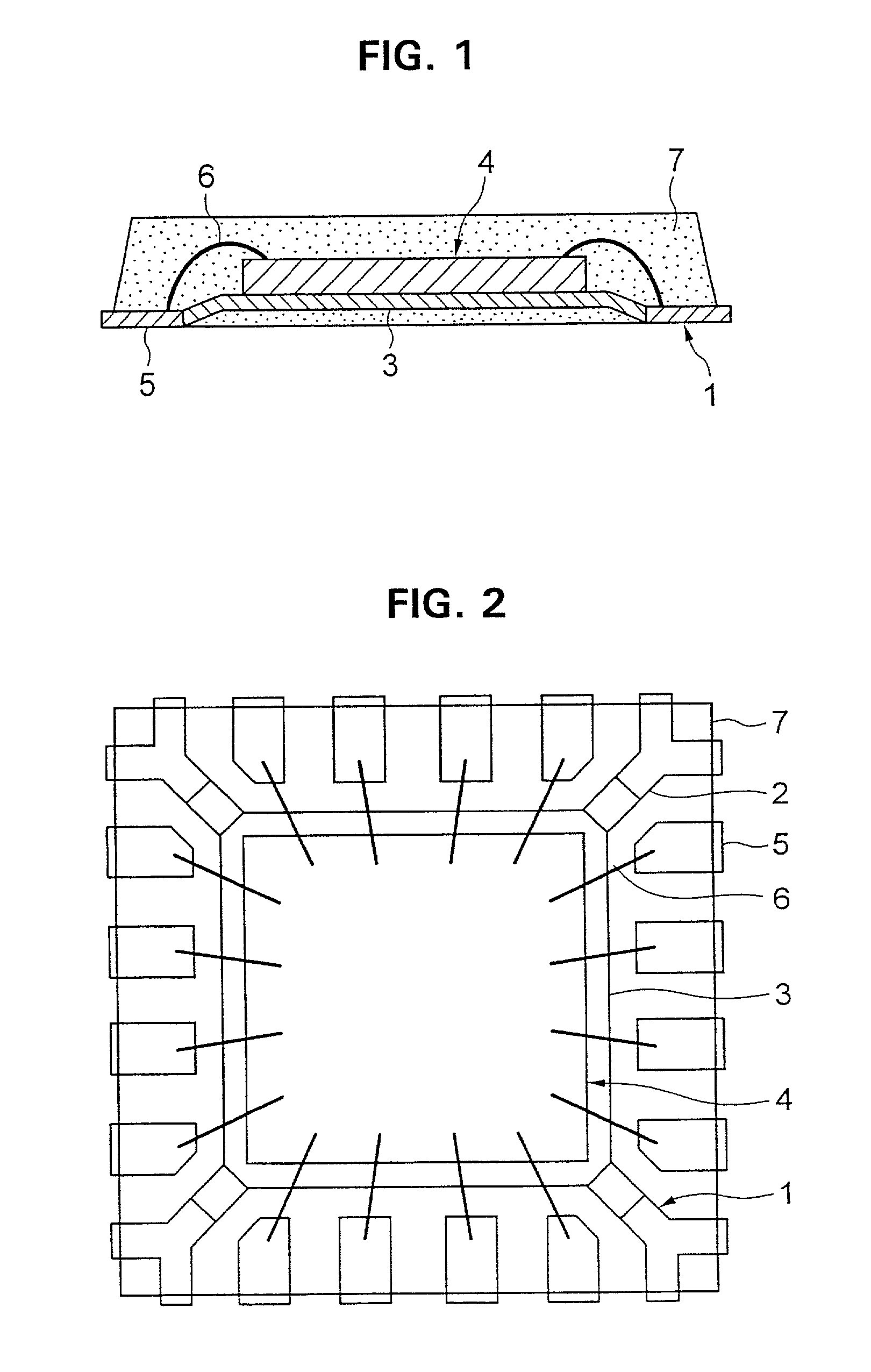
[0023] Then, referring to figures, embodiments of the present invention are explained.
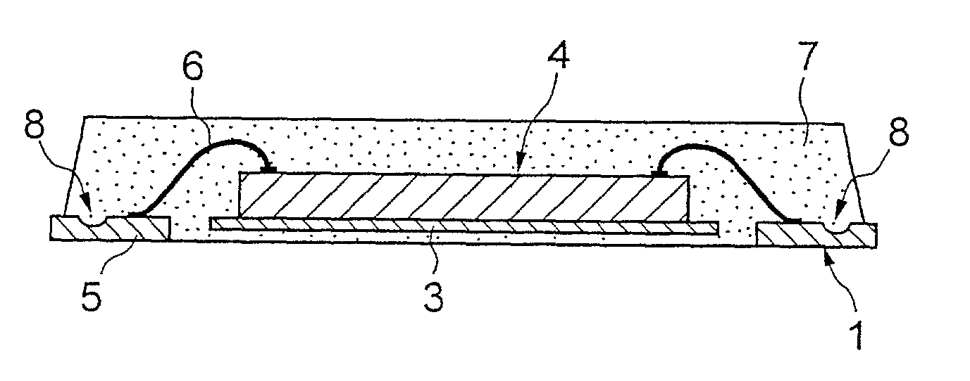
[0024] Lead frame 1 shown in FIGS. 5 and 6 is used for the production of an individually molding type of semiconductor, wherein a die-pad 3 is supported by four suspending leads 2 and four terminals 5 are projected from each of four peripheral sides of lead frame toward the die-pad 3, respectively. Each of terminals 5 has a groove 8 formed by half-etching the front side of terminals 5 at a given distance from the inside of each terminal 5. Further, in the lead frame shown in FIGS. 5 and 6, the backside of die-pad 3 is half-etched so that a thin die-pad is formed.
[0025] The lead frame 1 is made of cupper sheet with thickness of 0.2 mm, in case of almost illustrations. From a view point of the strength of terminals 5, grooves 8 formed by half-etching have a width of about 0.05 mm to 0.15 mm and a depth of about 25 to 75 per cent of the thickness of terminals 5, wherein a groove having a depth of abou...
PUM
| Property | Measurement | Unit |
|---|---|---|
| Adhesion strength | aaaaa | aaaaa |
| Area | aaaaa | aaaaa |
| Stress optical coefficient | aaaaa | aaaaa |
Abstract
Description
Claims
Application Information
 - Generate Ideas
- Intellectual Property
- Life Sciences
- Materials
- Tech Scout
- Unparalleled Data Quality
- Higher Quality Content
- 60% Fewer Hallucinations
Browse by: Latest US Patents, China's latest patents, Technical Efficacy Thesaurus, Application Domain, Technology Topic, Popular Technical Reports.
© 2025 PatSnap. All rights reserved.Legal|Privacy policy|Modern Slavery Act Transparency Statement|Sitemap|About US| Contact US: help@patsnap.com