

Phosphor thin film, preparation method, and EL panel
- Summary
- Abstract
- Description
- Claims
- Application Information
AI Technical Summary
Problems solved by technology
Method used
Image

Examples
example 1
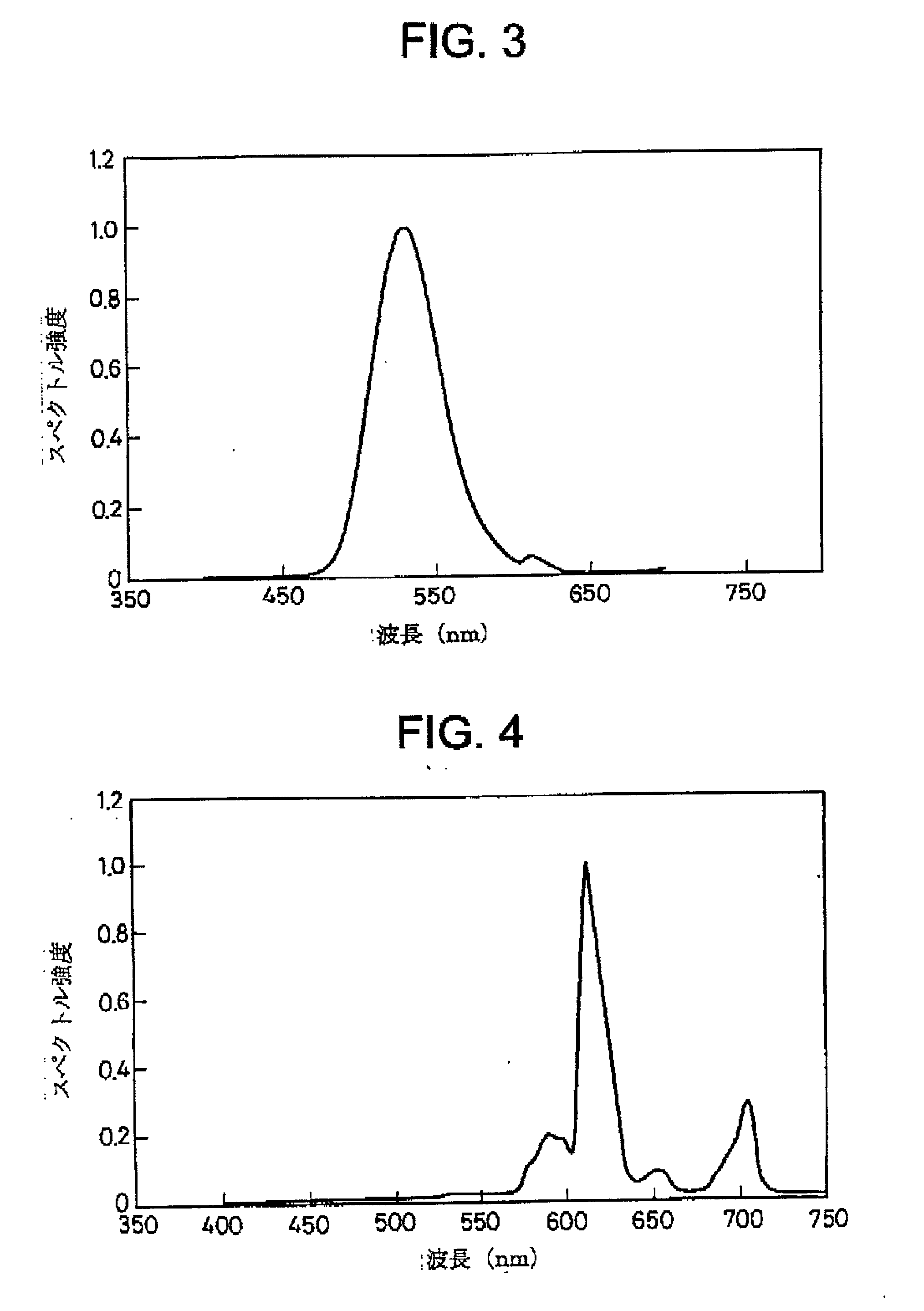
[0102] An EL device was fabricated using a phosphor thin film according to the invention.
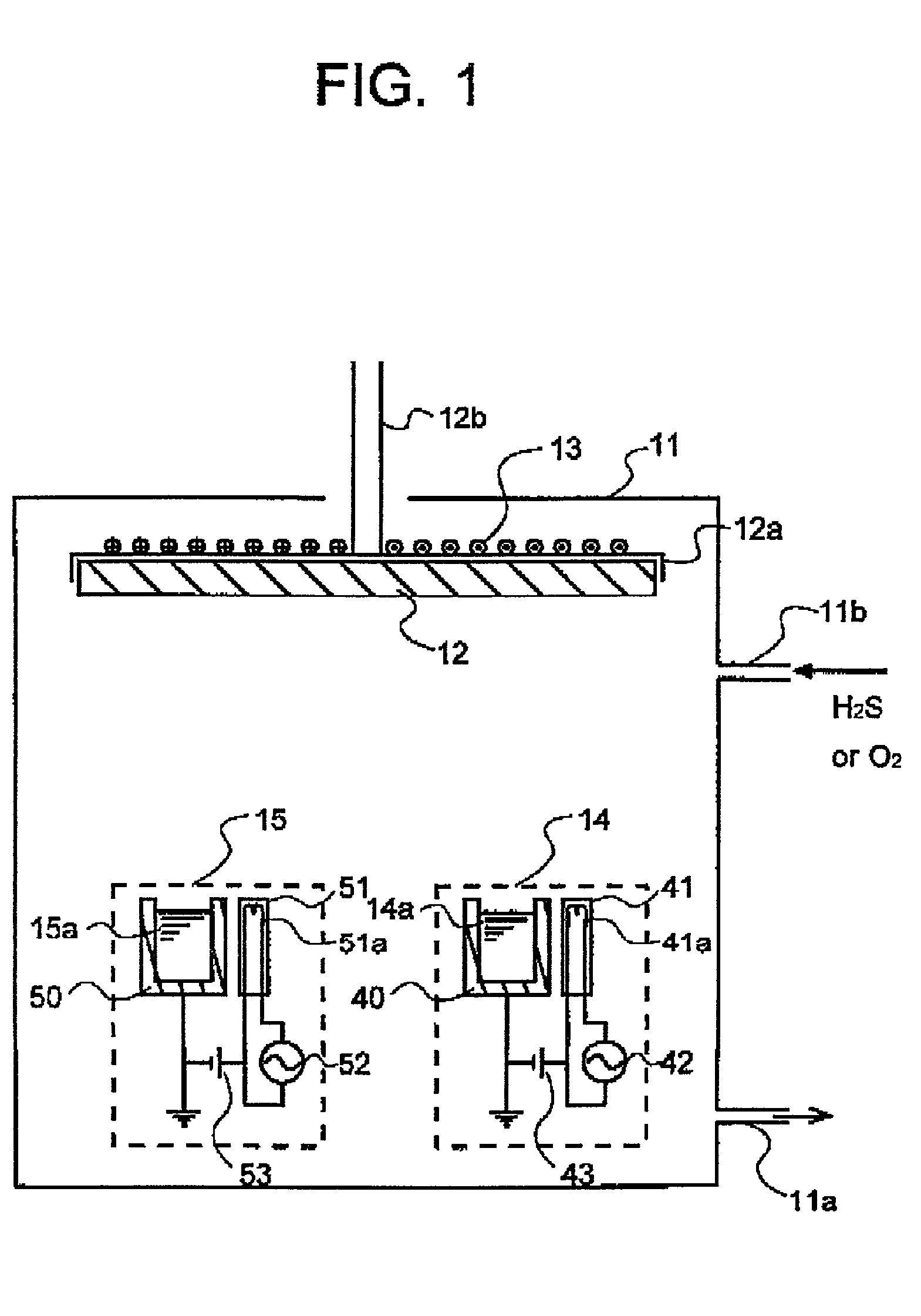
[0103] For both the substrate and the thick-film insulating layer, a BaTiO.sub.3 base dielectric material having a permittivity of 5,000 was commonly used. A Pd electrode was used as the lower electrode. The device was fabricated by furnishing a sheet for the substrate, and forming the lower electrode and thick-film insulating layer on the sheet by a screen printing technique to form a green sheet, followed by co-firing. The surface was polished, yielding a substrate bearing a thick-film first insulating layer of 30 .mu.m thick. A BaTiO.sub.3 film of 400 nm thick was formed thereon as a buffer layer by sputtering. This was annealed in air at 700.degree. C., yielding a composite substrate.
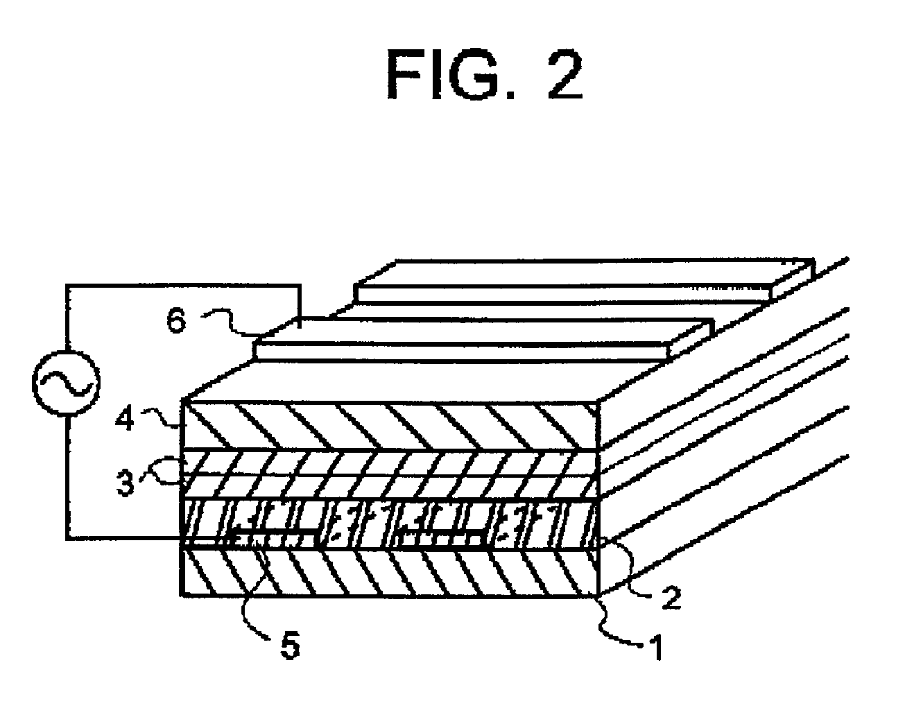
[0104] On the composite substrate, a structure of Al.sub.2O.sub.3 film 50 nm / ZnS film 200 nm / phosphor thin film (light emitting layer) 300 nm / ZnS film 200 nm / Al.sub.2O.sub.3 film 50 nm was formed so that the res...
example 2
[0110] In Example 1, terbium (Tb) was used instead of Eu as the rare earth element, providing emission of green light at a luminance of 53 cd / m.sup.2.
example 3
[0111] In Example 1, indium (In) was used instead of Ga, and praseodymium (Pr) was used instead of Eu as the rare earth element. Equivalent results were obtained, with emission of red light.
PUM
| Property | Measurement | Unit |
|---|---|---|
| Luminescence | aaaaa | aaaaa |
Abstract
Description
Claims
Application Information