Method and apparatus for inspecting a substrate

a substrate and substrate technology, applied in the direction of mechanical roughness/irregularity measurement, semiconductor/solid-state device testing/measurement, instruments, etc., can solve the problem of system reporting a defect, unable to distinguish real defects from false or nuisance defects, and prior art methods that do not recognize or recognize the advantage of combining more than two data sets

Active Publication Date: 2002-10-31
KLA TENCOR TECH CORP
View PDF25 Cites 89 Cited by
  • Summary
  • Abstract
  • Description
  • Claims
  • Application Information

AI Technical Summary

Problems solved by technology

If the difference equals or exceeds the threshold, the system reports a defect.
One significant weakness of the method disclosed by the prior art is that it attempts to distinguish real defects from false or nuisance defects on the basis of data from a single detector.
This prior art method doesn't acknowledge or recognize any advantage to be gained from combining more than two data sets in innovative ways before defining a defect.
As a result, the prior art doesn't ameliorate the difficult tradeoff between sensitivity and false defects.
Furthermore, it lends the operator very little flexibility in terms of his ability to look selectively for certain defect types.
None of the aforementioned prior art methods takes full advantage of the capabilities of a multi-detector SEM to inspect substrates.

Method used


Image

  • Method and apparatus for inspecting a substrate
  • Method and apparatus for inspecting a substrate
  • Method and apparatus for inspecting a substrate

Examples


Embodiment Construction

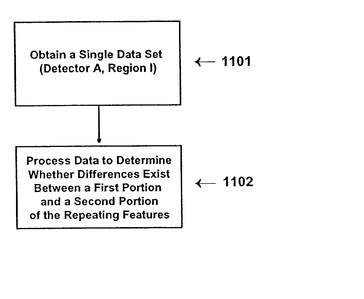
[0058] The following examples illustrate a variety of preferred methods and apparatus for for inspecting, redetecting, and / or classifying defects with an inspection system that exposes substrates to charged particles, detects the charged particles emitted from or scattered by the substrates, and processes the data.

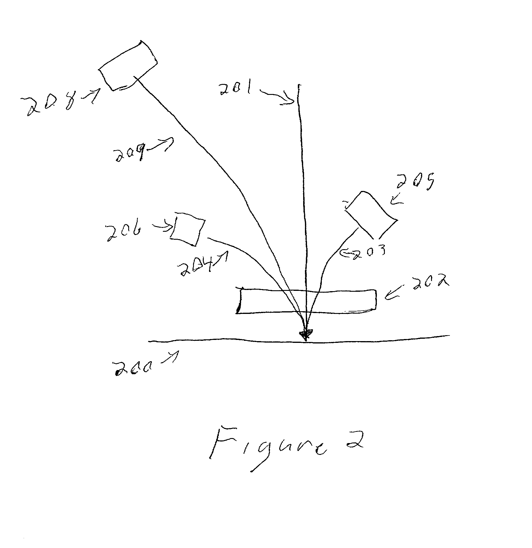
[0059] FIG. 2 illustrates an apparatus of an embodiment of the invention including a plurality of detectors. In this apparatus, electrons from incident beam 201 impinge upon substrate 200 and cause secondary and / or backscattered electrons 203 and 204 to be emitted from the substrate. Detectors 205 and 206 are used to detect electrons 203 and 204. Detectors 205 and 206 may be positioned so that one detects primarily secondary electrons, while the other detects primarily backscattered electrons. Alternatively, both detectors may detect secondary electrons, or both detectors may detect backscattered electrons. Selection of secondary electrons or backscattered electrons may be...


PUM

PropertyMeasurementUnit
diameteraaaaaaaaaa
azimuthal angleaaaaaaaaaa

Abstract

A method and apparatus for inspection and review of defects is disclosed wherein data gathering is improved. In one embodiment, multiple or segmented detectors are used in a particle beam system.

Description

[0001] This application claims priority to U.S. Provisional Patent Application Serial No. 60 / 256168, filed Dec. 15, 2000, the disclosure of which is hereby incorporated by reference.[0002] To achieve high manufacturing yields, the semiconductor industry depends on careful inspections of photomasks, bare silicon wafers, and processed silicon wafers. The inspection requirements are becoming more stringent as the industry inscribes smaller features on each new generation of integrated circuits. The resolution of optical inspection systems is becoming inadequate to find the small defects which can spoil the performance of an integrated circuit. To find smaller defects, the industry will increasingly rely on electron-beam inspection systems and review stations, which offer at least 10 times better resolution than optical systems. These inspection systems are variations on the traditional scanning electron microscope. Such inspection systems and review stations may, of course, find use in...

Claims


Application Information

Patent Timeline
Patent Type & Authority Applications(United States)
IPC IPC(8): G01N21/956G01N23/20G01N23/225G03F1/00G03F7/20H01J37/22H01J37/28H01L21/66
CPCG01N21/956G01N21/95607G01N23/20G01N23/2252H01J2237/2817G03F1/86G03F7/70616G03F7/7065H01J37/28G03F1/84G01N23/203G01N23/2251G01N2223/304G01N2223/611G01N2223/646H01J37/244
Inventor ADLER, DAVIDBERTSCHE, KIRKMCCORD, MARKFRIEDMAN, STUART
Owner KLA TENCOR TECH CORP
Why Eureka
Try Eureka