Self-aligned corner Vt enhancement with isolation channel stop by ion implantation

a self-aligning, corner vt technology, applied in the manufacturing of semiconductor/solid-state devices, basic electric elements, electric devices, etc., can solve the problems of sub-vt leakage, overall degradation of chip yield and performance, and degraded corner threshold voltage (vt) of fet devices

Inactive Publication Date: 2002-12-05
IBM CORP
View PDF0 Cites 14 Cited by
  • Summary
  • Abstract
  • Description
  • Claims
  • Application Information

AI Technical Summary

Problems solved by technology

The corner threshold voltage (Vt) of FET devices is degraded by several process related issues such as the corner rounding of the silicon at the edge of the device, wrap-around of the gate conductor, and the thinning of the gate oxide.
The resultant lowering of the corner Vt contributes to sub-Vt leakage and an overall degradation of chip yield and performance.
Corner Vt degradation has been addressed by engineering the radius of curvature of the silicon at the edge of the device; however, this has produced only modest recovery of Vt.
Corner Vt degradation has been mitigated by the introduction of oxidation catalysts like potassium, but such mobile ions are diffi

Method used


Image

  • Self-aligned corner Vt enhancement with isolation channel stop by ion implantation
  • Self-aligned corner Vt enhancement with isolation channel stop by ion implantation
  • Self-aligned corner Vt enhancement with isolation channel stop by ion implantation

Examples


Embodiment Construction

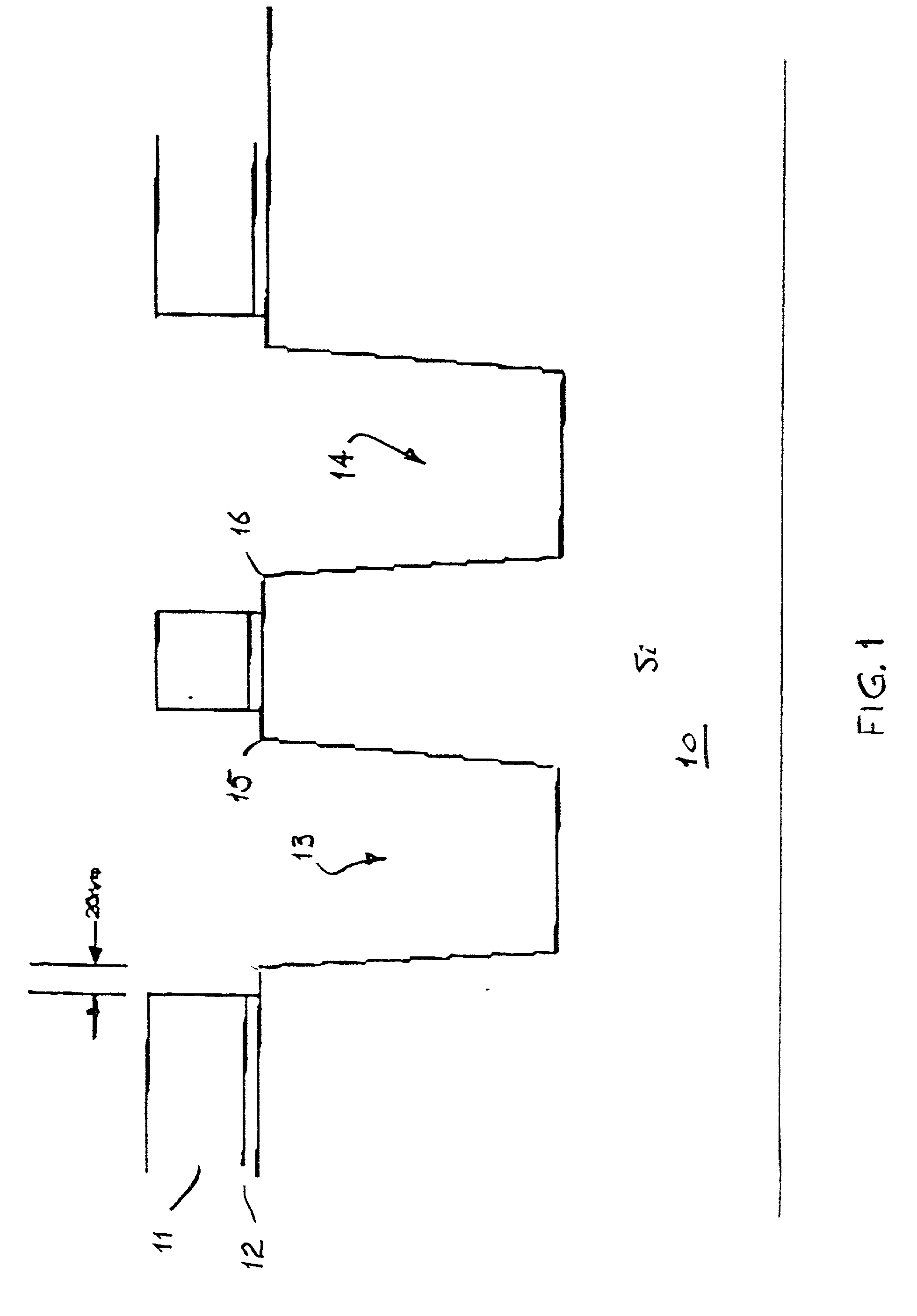
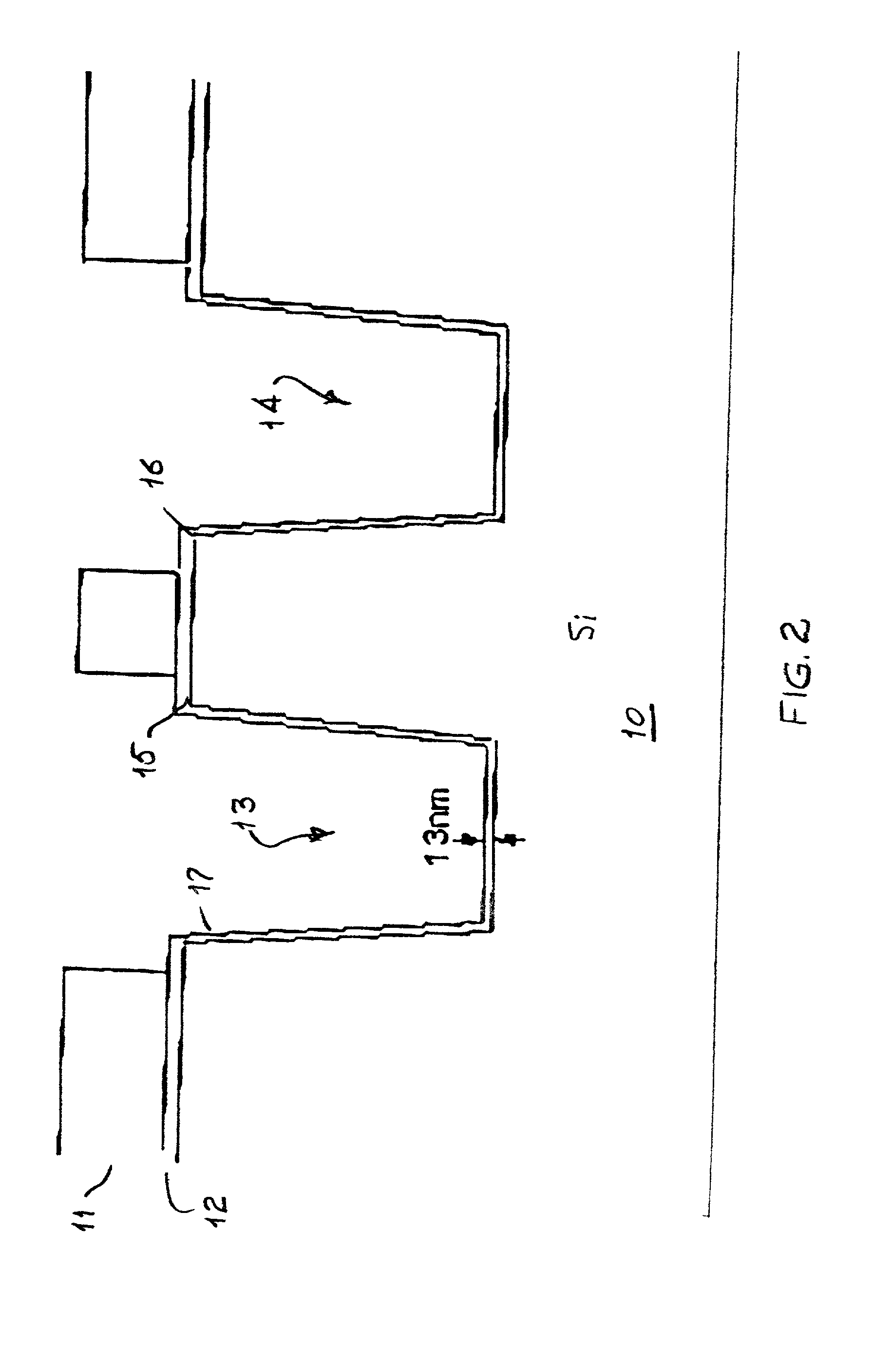
[0015] Referring now to the drawings, and more particularly to FIG. 1, there is shown in cross-sectional view the first step in the manufacture of an FET device according to the invention. A silicon substrate 10 is prepared by first depositing a layer of silicon dioxide 11 and then a layer of silicon nitride 12. Trenches 13 and 14 are formed in silicon substrate 10 by using a photolithiographic process to define the trenches in a photoresist applied to the silicon nitride layer 12 and then etching the trenches through the exposed silicon nitride and silicon dioxide layers into the silicon substrate as is conventional in the art. These trenches will be used to provide STI for the FET device. Next, the photoresist used to define the trenches 13 and 14 is removed, and the silicon nitride and silicon dioxide layers 12 and 11 are pulled back on the wafer surface to leave exposed edges 15 and 16. In the example shown, 120 nm of silicon nitride and 5 nm of silicon dioxide are simultaneousl...


PUM


Abstract

A process of fabricating a field effect transistor (FET) device uses the simultaneous implantation of the well species at the edge of the device and at the bottom of the shallow trench isolation (STI). This not only simplifies the process by defining the region for implantation at the device edge and at the bottom of the isolation with a single photo masking level, it also avoids the dual problems of corner Vt degradation and leakage across the bottom of the isolation trench. By implantation of the well species into the corner of the device region, the degradation of the corner Vt is mitigated by the additional channel doping in the edge of the device. The leakage across the bottom of the STI is eliminated by the simultaneous implantation of the well species at the interface thus raising the dopant level of the parasitic channel.

Description

[0001] 1. Field of the Invention[0002] The present invention generally relates to the fabrication of field effect transistor (FET) devices and, more particularly, to a process which avoids the dual problems of corner threshold voltage (Vt) degradation and leakage across the bottom of the isolation trench while at the same time realizing certain economies by simplifying the manufacturing process.[0003] 2. Background Description[0004] The corner threshold voltage (Vt) of FET devices is degraded by several process related issues such as the corner rounding of the silicon at the edge of the device, wrap-around of the gate conductor, and the thinning of the gate oxide. The resultant lowering of the corner Vt contributes to sub-Vt leakage and an overall degradation of chip yield and performance. Corner Vt degradation has been addressed by engineering the radius of curvature of the silicon at the edge of the device; however, this has produced only modest recovery of Vt. Corner Vt degradati...

Claims


Application Information

Patent Timeline
IPC IPC(8): H01L21/762
CPCH01L21/76237
Inventor GOTH, GEORGE R.KIM, JOHNNASTASI, VICTOR R.
Owner IBM CORP
Why Eureka
Try Eureka