

Magnetoresistive element, memory element having the magnetoresistive element, and memory using the memory element
a memory element and magnetoresistive element technology, applied in the field of magnetoresistive element, memory element having the magnetoresistive element, and memory using the memory element, can solve the problems of long erase time, no memory which satisfies all specifications, volatile and loses information upon power-off,
Inactive Publication Date: 2002-12-05
CANON KK
View PDF5 Cites 16 Cited by
- Summary
- Abstract
- Description
- Claims
- Application Information
AI Technical Summary
Problems solved by technology
There is no memory which satisfies all specifications required by current information devices.
For example, the DRAM achieves high recording density and large rewritable count, but is volatile and loses its information upon power-off.
The flash EEPROM is nonvolatile, but takes a long erase time and is not suitable for high-speed information processing.
As the element is downsized for a higher recording density of an MRAM, the MRAM using an in-plane magnetization film becomes more difficult to hold information under the influence of a demagnetizing field or magnetization curling at the end face.
This method cannot downsize the element, so an increase in recording density cannot be expected.
Especially in a memory used in a portable terminal, supply of a large current is undesirably flowed under restrictions on the power supply capacity.
This measure complicates a structure or electrical circuit around the magnetoresistive film, and is difficult to form.
This results in low yield and very high cost.
Needless to say, an actual magnetization switching behavior is a microscopic, complicated reaction based on micromagnetics.
At an energy of 10 keV or less, no satisfactory transformation occurs.
At an energy over 300 keV, a target object is physically damaged and may be destructed.
Method used
View moreImage
Smart ImageViewing Examples

Examples
Embodiment Construction
.62
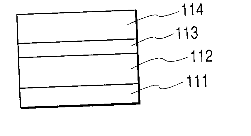
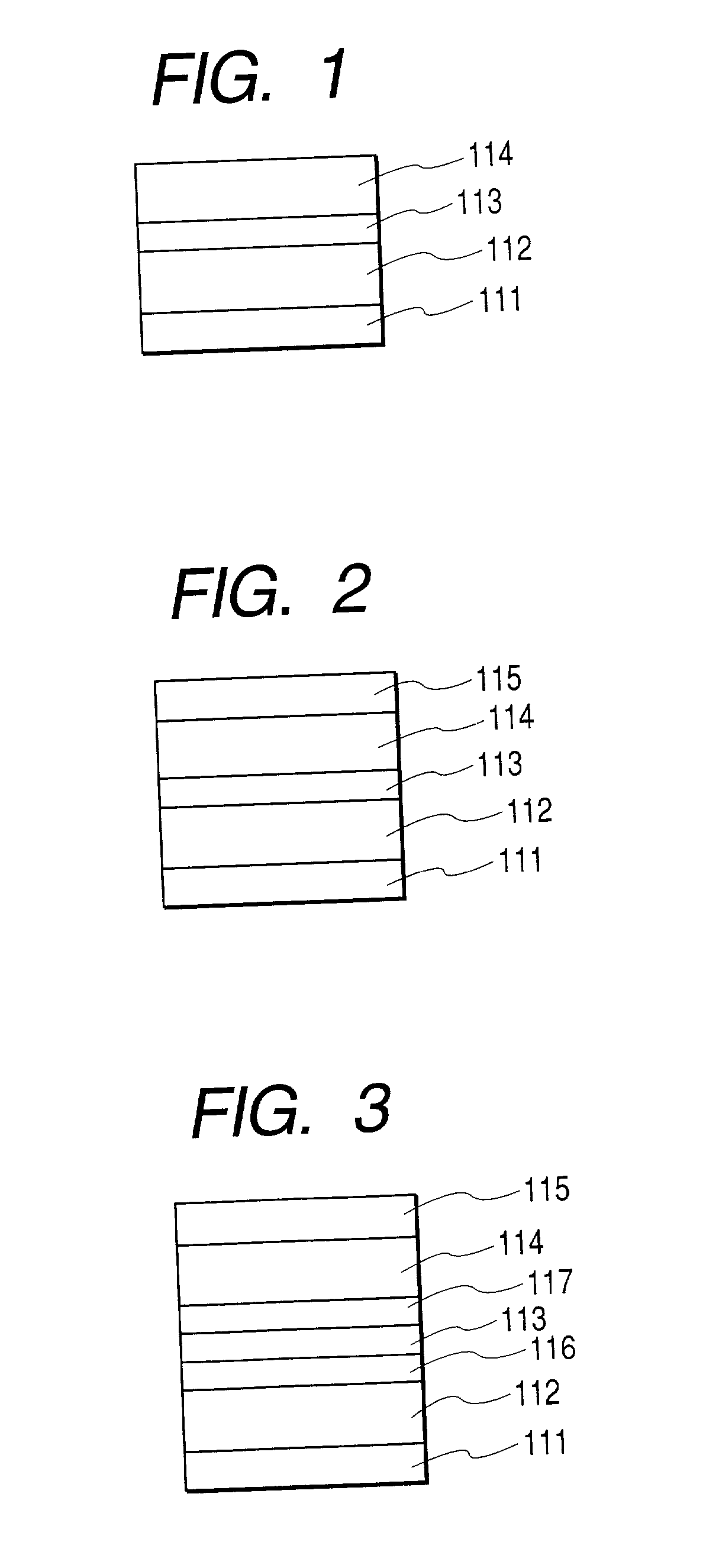
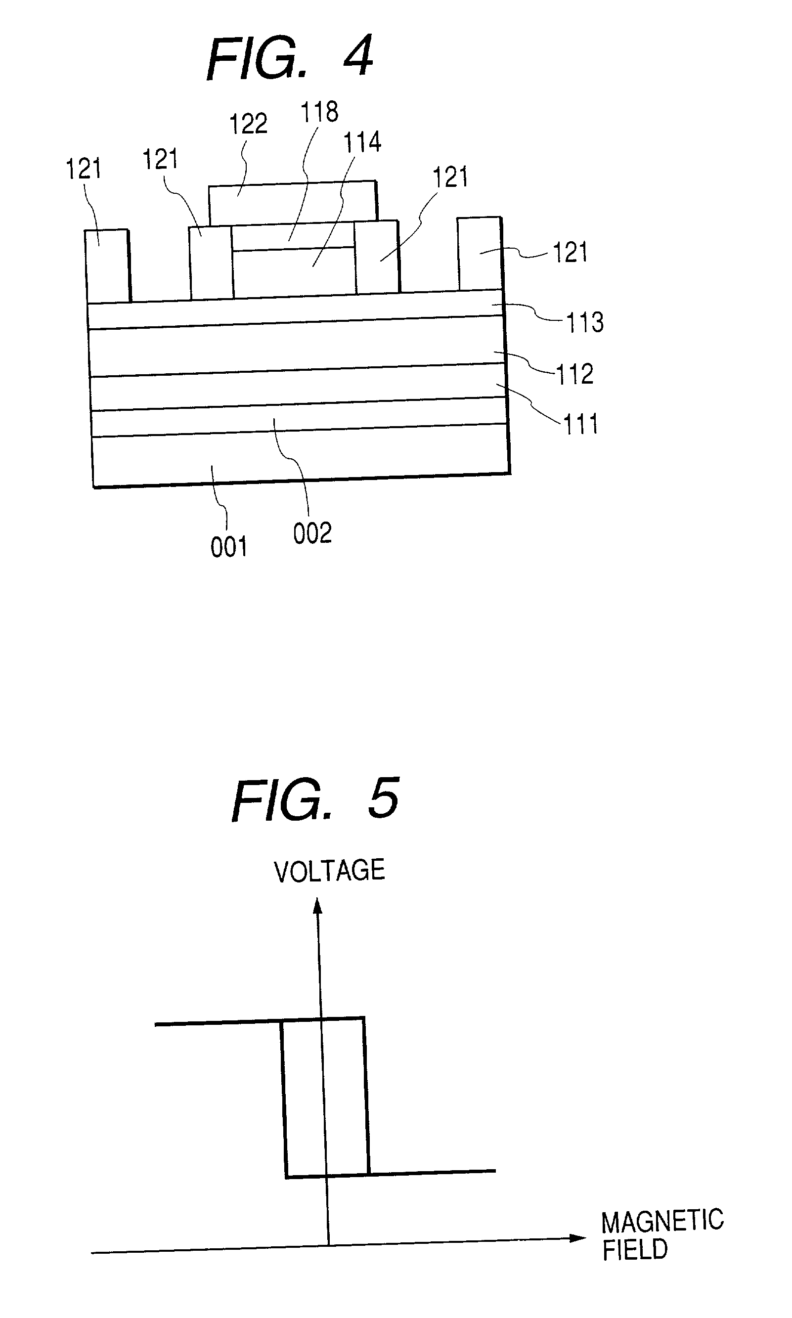
[0156] The present invention is not limited to the embodiments described above, and may be practiced by combining a plurality of embodiments. A tunneling magnetoresistive element suitably used for an MRAM has been exemplified as a magnetoresistive element. However, the present invention is not limited to this, and the structure of the present invention can also be applied to, e.g., a giant magnetoresistive element in which a nonmagnetic layer is made of a conductor.
Login to View More PUM
| Property | Measurement | Unit |
|---|---|---|
| Length | aaaaa | aaaaa |
| Length | aaaaa | aaaaa |
| Length | aaaaa | aaaaa |
Abstract
A magnetoresistive film includes a nonmagnetic film, and a structure in which magnetic films are formed on the two sides of the nonmagnetic film. At least one of the magnetic films is a perpendicular magnetization film. A magnetic film whose easy axis of magnetization is inclined from a direction perpendicular to the film surface is formed at a position where the magnetic film contacts the perpendicular magnetization film but does not contact the nonmagnetic film. A memory, magnetic element, magnetoresistive element, and magnetic element manufacturing method are also disclosed.
Description
[0001] 1. Field of the Invention[0002] The present invention relates to a magnetoresistive element using a method of reducing magnetic field inverting magnetization thereinafter, referred to as switching field of a magnetic film, a memory element having the magnetoresistive element, and a memory using the memory element.[0003] 2. Related Background Art[0004] In recent years, semiconductor memories as solid-state memories are adopted in many information devices, and are of various types such as a DRAM, FeRAM, and flash EEPROM. The characteristics of the semiconductor memories have merits and demerits. There is no memory which satisfies all specifications required by current information devices. For example, the DRAM achieves high recording density and large rewritable count, but is volatile and loses its information upon power-off. The flash EEPROM is nonvolatile, but takes a long erase time and is not suitable for high-speed information processing.[0005] Under the present circumstan...
Claims
Login to View More Application Information
Patent Timeline
 IPC IPC(8): G11C11/16G11C11/15
CPCG11C11/16Y10T428/1121Y10T428/24942Y10T428/1107Y10T428/12986Y10T428/1143Y10T428/12465G11C11/161H10N50/10H10N50/01G11C11/15
InventorIKEDA, TAKASHIKOGANEI, AKIOOKANO, KAZUHISA
OwnerCANON KK