Spin Transistor Using Perpendicular Magnetization

a technology of perpendicular magnetization and spin transistor, which is applied in the direction of digital storage, semiconductor devices, instruments, etc., can solve the problems of physical limitation of gate oxide layers, difficult to reduce power consumption and area,

Inactive Publication Date: 2008-12-18
KOREA INST OF SCI & TECH
View PDF7 Cites 18 Cited by
  • Summary
  • Abstract
  • Description
  • Claims
  • Application Information

AI Technical Summary

Benefits of technology

[0008]An aspect of the present invention provides a spin transistor useful for device miniaturization and high-density integration and capable of controlling resistance by using a gate.

Problems solved by technology

In the MOSFET used as a basic component in the current semiconductor devices, a voltage of the MOSFET is written and read by charging and discharging of charges, so that power consumption and area are difficult to reduce.
In addition, there is a physical limitation to a gate oxide layer.

Method used


Image

  • Spin Transistor Using Perpendicular Magnetization
  • Spin Transistor Using Perpendicular Magnetization
  • Spin Transistor Using Perpendicular Magnetization

Examples


Embodiment Construction

[0025]Hereinafter, exemplary embodiments of the present invention will now be described in detail with reference to the accompanying drawings. The embodiments of the present invention may be modified in various forms, and the scope of the present invention is not limited to the embodiments. The embodiments of the present invention are provided in order that the ordinarily skilled in the art can have the better understanding of the present invention.

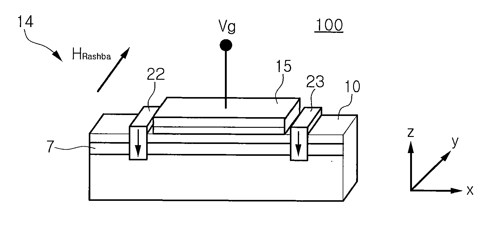
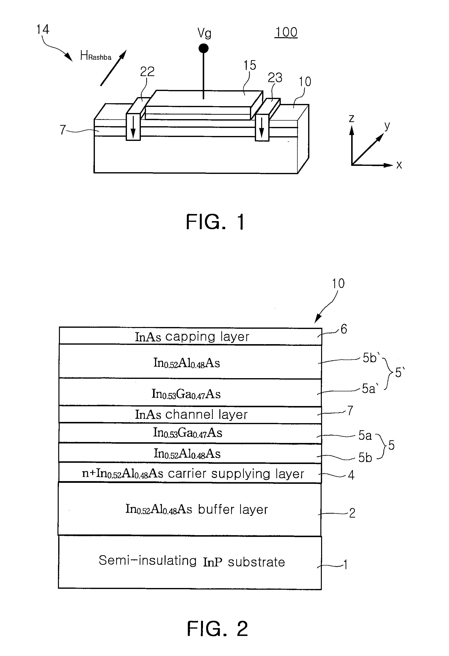
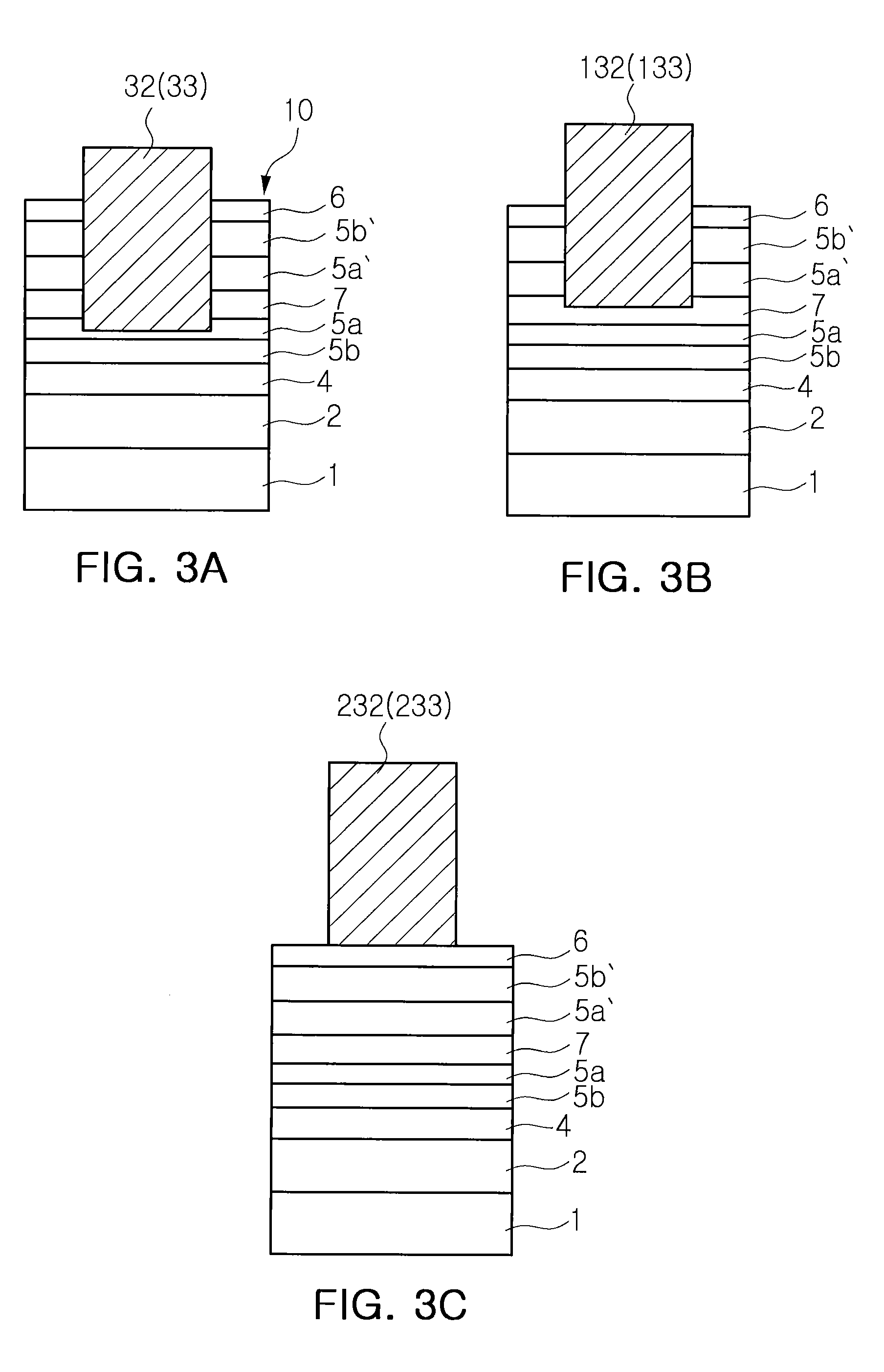
[0026]FIG. 1 is a perspective view illustrating a spin transistor according to an embodiment of the present invention. Referring to FIG. 1, the spin transistor 100 includes a semiconductor substrate 10 having a channel layer 7 and a ferromagnetic source 22 and a ferromagnetic drain 23 which are disposed on the semiconductor substrate 10 to be separated from each other. A gate 15 is disposed on the semiconductor substrate 10 between the source 22 and the drain 23. The gate 15 is insulated from the source 22, the drain 23, and the semicondu...


PUM


Abstract

A spin transistor useful for device miniaturization and high-density integration is provided. The spin transistor includes: a semiconductor substrate including a channel layer; ferromagnetic source and drain disposed on the semiconductor substrate to be separated from each other and to be magnetized in a direction perpendicular to a surface of the channel layer; a gate formed on the semiconductor substrate between the source and the drain to adjust spins of electrons passing through the channel layer, wherein spin-polarized electrons are injected from the source to the channel layer, and the electrons injected into the channel layer pass though the channel layer and are injected into the drain, and wherein the spins of the electrons passing through the channel layer undergo precession due to a spin-orbit coupling induced magnetic field according to a voltage of the gate.

Description

CROSS-REFERENCE TO RELATED APPLICATIONS[0001]This application claims the priority of Korean Patent Application No. 2007-58532 filed on Jun. 14, 2007, in the Korean Intellectual Property Office, the disclosure of which is incorporated herein by reference.BACKGROUND OF THE INVENTION[0002]1. Field of the Invention[0003]The present invention relate to a spin transistor, and more particularly, to a spin transistor useful for device miniaturization and high-density integration.[0004]2. Description of the Related Art[0005]In an integrated circuit (IC) technology, a metal oxide semiconductor field effect Transistor (MOSFET) has been widely used as a basic component for various electronic devices. For example, a memory device such as a dynamic random access memory (DRAM) and a flash memory, an application specific integrated circuit (ASIC) device, a microprocessor, a logic circuit, and the like have been operated by on / off operations of the MOSFET. Recently, as a substitute for the MOSFET, a...

Claims


Application Information

Patent Timeline
Patent Type & Authority Applications(United States)
IPC IPC(8): H01L29/96
CPCG11C11/16H01L29/20H01L29/66984H01L27/105H01L29/82
Inventor KOO, HYUN-CHEOLHAN, SUK-HEECHANG, JOON-YEONKIM, HYUNG-JUNMA, JIN-SEOCK
Owner KOREA INST OF SCI & TECH
Why Eureka
Try Eureka