Variable salicide block for resistance equalization in an array

a salicide block and array technology, applied in the field of memory devices, can solve the problems of affecting programming, erasing and reading of memory devices, memory losing data, and reducing data storage density,

Inactive Publication Date: 2010-05-11
MONTEREY RES LLC
View PDF0 Cites 6 Cited by
  • Summary
  • Abstract
  • Description
  • Claims
  • Application Information

AI Technical Summary

Benefits of technology

[0021]One aspect of the present invention facilitates memory devices and operation of dual bit and single bit memory devices by providing systems and methods that can employ a non-symmetrical salicide block, for example, for resistance equalization of the memory array during fabrication. Employment of the salicide block facilitates dual bit and single bit memory device operation by mitigating charge-loss and contact resistance while providing protection against charge-up on the various lines from plasma etching processes. One example of the present invention includes utilizing a silicon rich nitride layer formed on a plurality of wordlines.
[0022]A further aspect of the present invention can utilize a common charge dissipation element to mitigate charge-loss by providing protection against charging up of the various lines as a result of further plasma etching processes. Alternatively, a common charge dissipation element provides a region of charge dissipation away from the memory array to prevent charge-up of the memory cell during processing or various etches.
[0023]Another aspect of the present invention utilizes a triangular wedge shaped salicide region for purposes of controlling the resistance of each wordline of an array to a common shorting element of a common discharge element. The salicide block equalizes the charge dissipation in the memory array by providing each wordline with a varied amount of resistance. Because the charge protection provided to each wordline varies depending on the total resistance path to a common discharge element, a varying shape salicide block for resistance equalization provides greater reliability and predictability during processing. Numerous such shapes, conducive for any desired resistance path fall within the scope of the invention, for example oval, trapezoidal, and the like. Any shape of the salicide block may be utilized by varying the measured angle or shape of etching on each wordline or calculated so that the resistance matches each wordline path to a common element.
[0026]Yet another aspect of the present invention comprises one or more common shorting paths connecting a plurality of wordlines to one or more discharge elements of a sector of an array. One example is a sector of an array being symmetrically aligned so that a common discharge element of a common shorting path is placed on each side of a shared plurality of wordlines, thereby facilitating charged line bleed-off from each end of a wordline into a common charge dissipation region. Other symmetrical or asymmetrical alignments of common charge dissipation elements within an array are also contemplated and within the scope of the present invention.

Problems solved by technology

For example, DRAM and SRAM allow individual bits of data to be erased one at a time, but such memory loses its data when power is removed.
EEPROM can alternatively be easily erased without extra exterior equipment, but has reduced data storage density, lower speed, and higher cost.
Charge loss is a loss of charge for memory cells over time that can cause a cell initially in one charge state to move to a different charge state.
Contact resistance is resistance at an interface between a formed contact and a wordline or bitline and can lead to undesired voltage drops across the interface that negatively impact programming, erasing, and reading of the memory device.
This could result in corrupt data and / or inaccurately stored or programmed data.
Similarly, other issues, such as leakage currents, cross talk, etc., can also result from scaling.
For example, isolating two bits or charges stored in a charge trapping layer becomes increasingly difficult as the channel length is decreased and the bits are brought closer together.

Method used


Image

  • Variable salicide block for resistance equalization in an array
  • Variable salicide block for resistance equalization in an array
  • Variable salicide block for resistance equalization in an array

Examples


Embodiment Construction

[0036]One or more aspects of the present invention are described with reference to the drawings, wherein like reference numerals are generally utilized to refer to like elements throughout, and wherein the various structures are not necessarily drawn to scale. In the following description, for purposes of explanation, numerous specific details are set forth in order to provide a thorough understanding of one or more aspects of the present invention. It may be evident, however, to one skilled in the art that one or more aspects of the present invention may be practiced with a lesser degree of these specific details. In other instances, well-known structures and devices are shown in block diagram form in order to facilitate describing one or more aspects of the present invention.

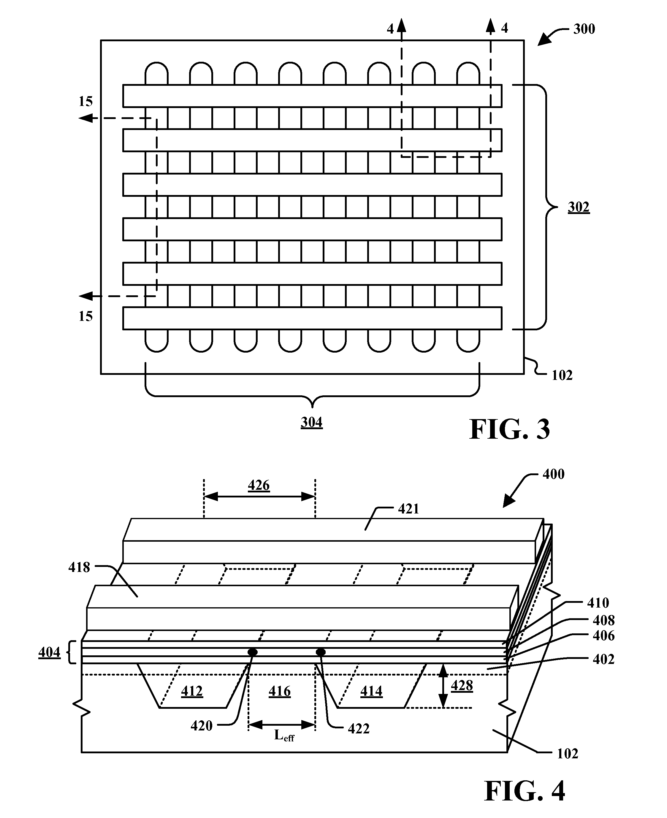
[0037]The present invention facilitates memory devices and operation of dual bit and single bit memory devices by providing systems and methods that employ a salicide block to vary and equalize the resistance ...


PUM


Abstract

The present invention facilitates memory devices and operation of dual bit and single bit memory devices by providing systems and methods that employ a salicide block to vary and equalize the resistance of a memory array during fabrication. The present invention includes utilizing a common charge dissipation region to mitigate charge-loss by providing protection against charging up of the various lines as a result of further plasma etching processes. The salicide block equalizes the charge dissipation in the memory array by providing each wordline path with a varied amount of resistance in addition to the total path resistance. Because the charge protection provided to each wordline otherwise varies depending on the resistance path to a common discharge element, a salicide block for resistance equalization provides greater reliability and predictability during processing. Other such shapes conducive for any desired resistance path fall within the scope of the invention.

Description

REFERENCE TO RELATED APPLICATIONS[0001]This application claims the benefit of U.S. Provisional Patent Application Ser. No. 60 / 875,905 which was filed Dec. 20, 2006, entitled “VARIABLE SALICIDE BLOCK FOR RESISTANCE EQUALIZATION IN AN ARRAY.”FIELD OF INVENTION[0002]The present invention relates generally to memory devices and the like, and in particular to fabricating dual bit and single bit memory devices with improved reliability to a commonly joined element by a variable salicide block equilibrating the resistance in an array.BACKGROUND OF THE INVENTION[0003]Many different types and styles of memory exist to store data for computers and similar type systems. For example, random access memory (RAM), dynamic random access memory (DRAM), static random access memory (SRAM), read only memory (ROM), programmable read only memory (PROM), electrically programmable read only memory (EPROM), electrically erasable programmable read only memory (EEPROM) and flash memory are all presently avail...

Claims


Application Information

Patent Timeline
Patent Type & Authority Patents(United States)
IPC IPC(8): H01L21/44
CPCH01L21/28282H01L21/76837H01L29/7923H01L27/11568H01L27/115H01L29/40117H10B43/30H10B69/00
Inventor BRENNAN, MICHAELHE, YIRANDOLPH, MARKKWAN, MING-SANG
Owner MONTEREY RES LLC
Why Eureka
Try Eureka