Semiconductor integrated circuit devices having contacts formed of single-crystal materials

a technology of integrated circuits and materials, applied in the direction of semiconductor devices, transistors, electrical equipment, etc., can solve the problems of reduced reliability, increased risk of transistor failure, and increased difficulty in forming contacts, so as to increase the thickness of the inter-layer dielectric through which the contacts are formed, increase the separation between bit line and word line, and increase the critical dimension of the resulting direct contacts

Active Publication Date: 2011-11-08
IMBERATEK LLC
View PDF8 Cites 4 Cited by
  • Summary
  • Abstract
  • Description
  • Claims
  • Application Information

AI Technical Summary

Benefits of technology

[0006]In this manner, the critical dimension of the resulting direct contacts is increased, and thus, the thickness of the inter-layer dielectric through which the contacts are formed can be increased. This, in turn, increases the separation between the bit line and word line of the resulting memory device, which has a direct effect on the bit line loading capacitance of the resulting device. In addition, the SEG layer of the direct contact can be used to effectively extend the channel length of the resulting transistor, since the source / drain regions can be formed in the SEG layer, leading to increased device integration.
[0007]Further, a low-resistance junction is provided at the boundary of the narrow bottom portion of the SEG layer and the underlying substrate. Although a p-n junction is formed at the junction of the top portion of the SEG layer and the above-lying conductive metal plug, the interface is relatively wider, and therefore, resistance of the upper junction can be controlled to acceptable values. Also, leakage current between the direct contact and the trench gate is manageable, since the lower portion of the direct contact has a reduced width, and is therefore made to be a relatively further distance from the top of the gate.

Problems solved by technology

The resulting direct contacts suffer from a number of limitations that become more problematic as devices are further integrated and operate at higher speeds and at lower voltage levels.
Under these conditions, the resulting transistor is more likely to fail, or otherwise will operate with reduced reliability.
Also, fabrication of such devices can result in reduced yield, and therefore fabrication costs can be increased.

Method used


Image

  • Semiconductor integrated circuit devices having contacts formed of single-crystal materials
  • Semiconductor integrated circuit devices having contacts formed of single-crystal materials
  • Semiconductor integrated circuit devices having contacts formed of single-crystal materials

Examples


Embodiment Construction

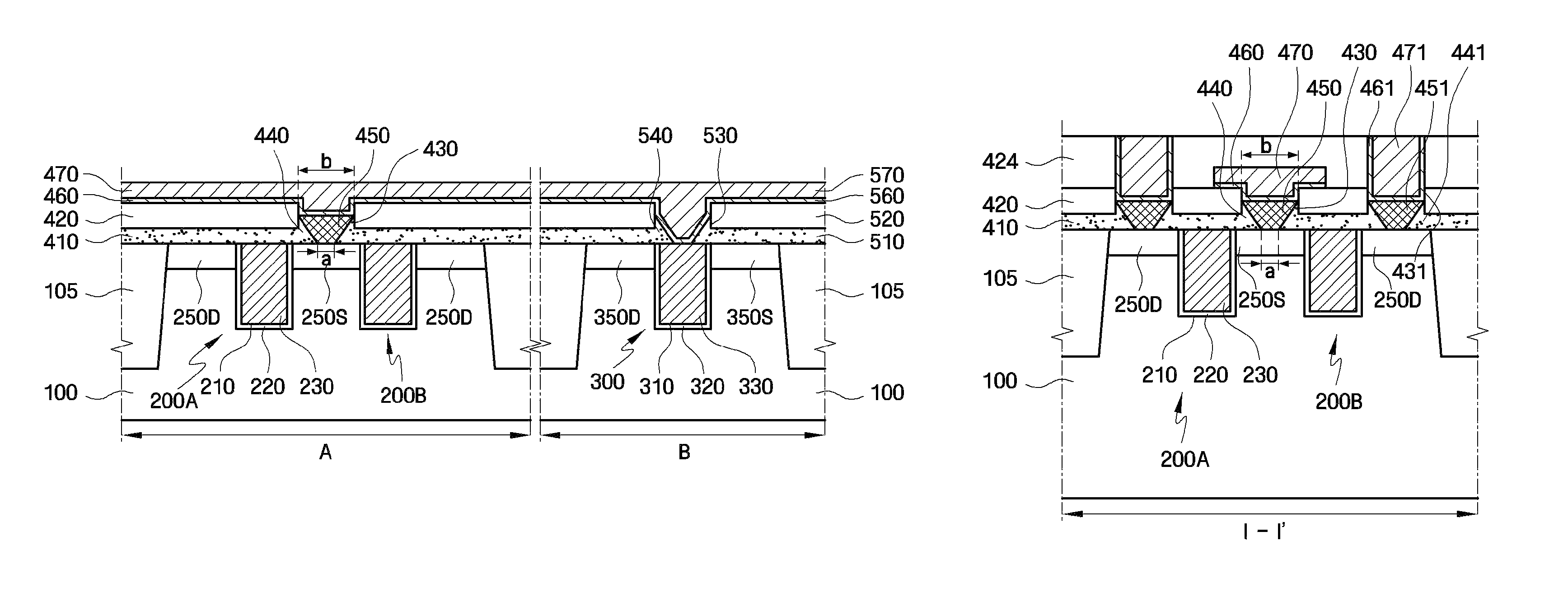
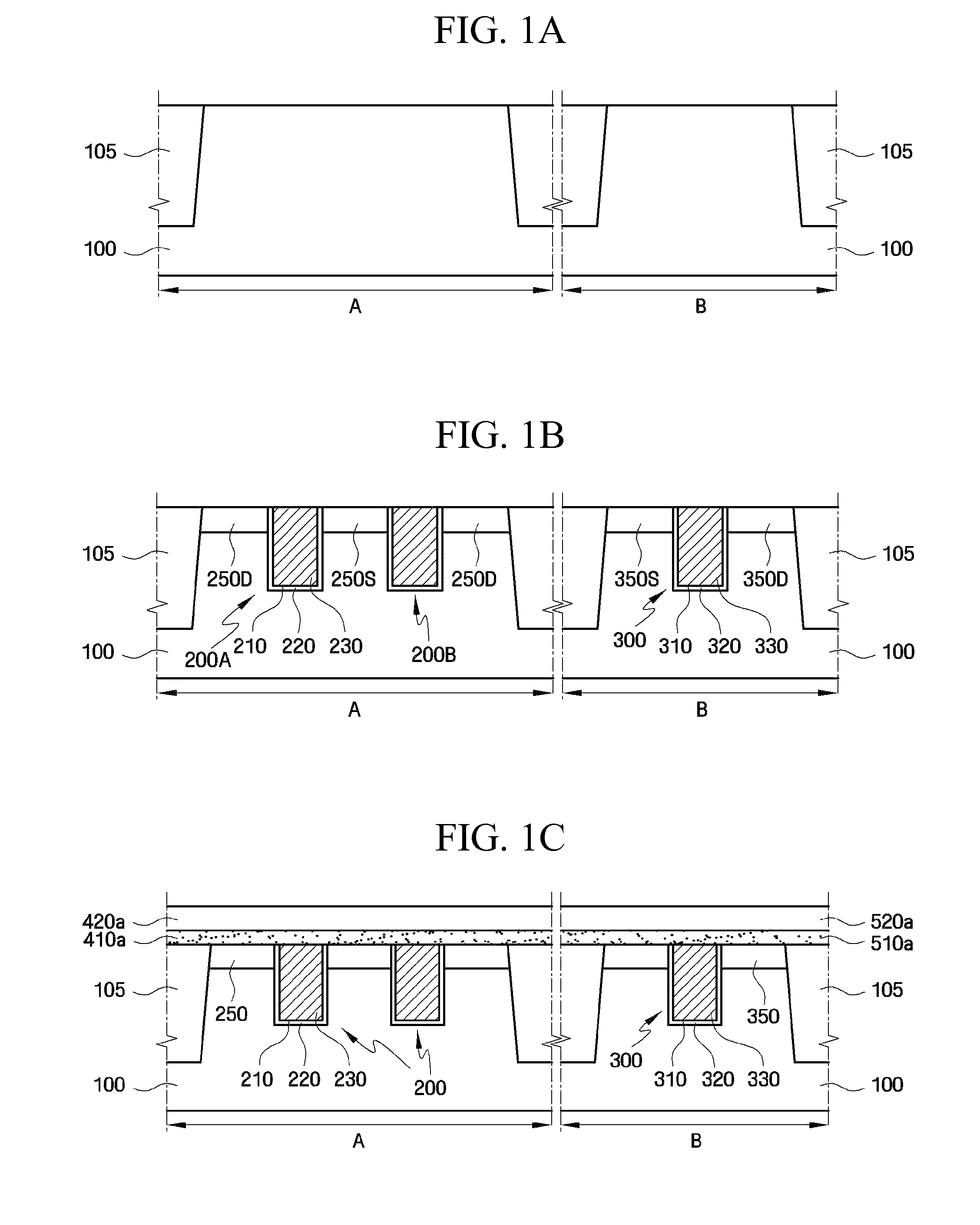
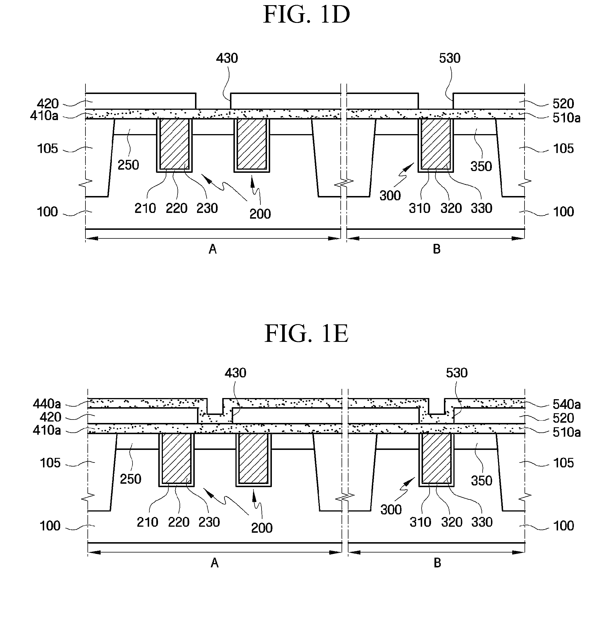
[0104]Embodiments of the present invention will now be described more fully hereinafter with reference to the accompanying drawings, in which preferred embodiments of the invention are shown. This invention may, however, be embodied in different forms and should not be construed as limited to the embodiments set forth herein. Like numbers refer to like elements throughout the specification.

[0105]It will be understood that, although the terms first, second, etc. are used herein to describe various elements, these elements should not be limited by these terms. These terms are used to distinguish one element from another. For example, a first element could be termed a second element, and, similarly, a second element could be termed a first element, without departing from the scope of the present invention. As used herein, the term “and / or” includes any and all combinations of one or more of the associated listed items.

[0106]It will be understood that when an element is referred to as b...


PUM


Abstract

A memory cell of memory device, comprises an active region of a memory cell defined in a semiconductor substrate, and a conductive gate electrode in a trench of the active region. The gate electrode is isolated from the semiconductor substrate. An insulation layer is on the active region and on the conductive gate electrode. A conductive contact is in the insulation layer on the active region at a side of the gate electrode and isolated from the gate electrode. The contact has a first width at a top portion thereof and a second width at a bottom portion thereof, the first width being greater than the second width. The contact is formed of a single-crystal material.

Description

RELATED APPLICATIONS[0001]This application claims priority under 35 U.S.C. 119 to Korean Patent Application No. 10-2007-0071321 filed on Jul. 16, 2007, the content of which is incorporated herein by reference in its entirety.BACKGROUND OF THE INVENTION[0002]Contemporary semiconductor memory devices commonly employ trench transistors in both memory cell regions and peripheral regions of a device. In a Buried Channel Array Transistor (BCAT) device, for example, a transistor gate is buried in a trench formed in a semiconductor substrate. The buried gate operates to extend the channel length of the resulting transistor structure, resulting in increased integration and greater reliability. Such trench transistors are disclosed, for example, in United States Patent Application Publication No. 2005 / 0127437, the contents of which are incorporated by reference in their entirety[0003]In a conventional trench transistor, a trench is formed in the substrate and the inner walls and base of the t...

Claims


Application Information

Patent Timeline
Patent Type & Authority Patents(United States)
IPC IPC(8): H01L29/66
CPCH01L21/28525H01L27/10876H01L27/10888H01L27/10894Y10S257/907Y10S257/905Y10S257/908Y10S257/906H10B12/053H10B12/485H10B12/09H01L21/28H01L21/18
Inventor YU, MAN-JONG
Owner IMBERATEK LLC
Why Eureka
Try Eureka